DF2214BQ16V Renesas Electronics America, DF2214BQ16V Datasheet - Page 528
DF2214BQ16V
Manufacturer Part Number
DF2214BQ16V
Description
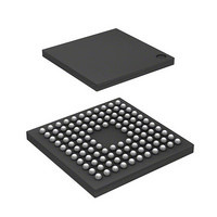
IC H8S/2214 MCU FLASH 112-TFBGA
Manufacturer
Renesas Electronics America
Series
H8® H8S/2200r
Datasheets
1.HS2214ECB62H.pdf
(938 pages)
2.HEWH8E10A.pdf
(19 pages)
3.D12312SVTE25V.pdf
(341 pages)
Specifications of DF2214BQ16V
Core Processor
H8S/2000
Core Size
16-Bit
Speed
16MHz
Connectivity
SCI
Peripherals
DMA, POR, PWM, WDT
Number Of I /o
72
Program Memory Size
128KB (128K x 8)
Program Memory Type
FLASH
Ram Size
12K x 8
Voltage - Supply (vcc/vdd)
2.7 V ~ 3.6 V
Data Converters
D/A 1x8b
Oscillator Type
Internal
Operating Temperature
-20°C ~ 75°C
Package / Case
112-TFBGA
For Use With
HS0005KCU11H - EMULATOR E10A-USB H8S(X),SH2(A)3DK2218 - DEV EVAL KIT H8S/2218
Lead Free Status / RoHS Status
Lead free / RoHS Compliant
Eeprom Size
-
Available stocks
Company
Part Number
Manufacturer
Quantity
Price
Company:

Part Number:
DF2214BQ16V
Manufacturer:
Renesas Electronics America
Quantity:
10 000


Section 12 Serial Communication Interface (SCI)
Bit 3
MPIE
0
1
Note: * When receive data including MPB = 0 is received, receive data transfer from RSR to RDR,
Bit 2—Transmit End Interrupt Enable (TEIE): Enables or disables transmit end interrupt
(TEI) request generation when there is no valid transmit data in TDR in MSB data transmission.
Bit 2
TEIE
0
1
Note: * TEI cancellation can be performed by reading 1 from the TDRE flag in SSR, then clearing
Bits 1 and 0—Clock Enable 1 and 0 (CKE1, CKE0): These bits are used to select the SCI clock
source and enable or disable clock output from the SCK pin. The combination of the CKE1 and
CKE0 bits determines whether the SCK pin functions as an I/O port, the serial clock output pin, or
the serial clock input pin.
The setting of the CKE0 bit, however, is only valid for internal clock operation (CKE1 = 0) in
asynchronous mode. The CKE0 bit setting is invalid in clocked synchronous mode, and in the case
of external clock operation (CKE1 = 1). Note that the SCI’s operating mode must be decided using
SMR after setting the CKE1 and CKE0 bits.
For details of clock source selection, see table 12.9.
Rev.4.00 Sep. 18, 2008 Page 466 of 872
REJ09B0189-0400
receive error detection, and setting of the RDRF, FER, and ORER flags in SSR , is not
performed. When receive data including MPB = 1 is received, the MPB bit in SSR is set to
1, the MPIE bit is cleared to 0 automatically, and generation of RXI and ERI interrupts
(when the TIE and RIE bits in SCR are set to 1) and FER and ORER flag setting is
enabled.
it to 0 and clearing the TEND flag to 0, or clearing the TEIE bit to 0.
Description
Multiprocessor interrupts disabled (normal reception performed)
[Clearing conditions]
•
•
Multiprocessor interrupts enabled *
Receive interrupt (RXI) requests, receive error interrupt (ERI) requests, and setting
of the RDRF, FER, and ORER flags in SSR are disabled until data with the
multiprocessor bit set to 1 is received.
Description
Transmit end interrupt (TEI) request disabled *
Transmit end interrupt (TEI) request enabled *
When the MPIE bit is cleared to 0
When MPB= 1 data is received
(Initial value)
(Initial value)
Related parts for DF2214BQ16V
Image
Part Number
Description
Manufacturer
Datasheet
Request
R

Part Number:
Description:
CONN SOCKET 2POS 7.92MM WHITE
Manufacturer:
Hirose Electric Co Ltd
Datasheet:

Part Number:
Description:
CONN SOCKET 4POS 7.92MM WHITE
Manufacturer:
Hirose Electric Co Ltd
Datasheet:

Part Number:
Description:
CONN SOCKET 5POS 7.92MM WHITE
Manufacturer:
Hirose Electric Co Ltd
Datasheet:

Part Number:
Description:
CONN SOCKET 3POS 7.92MM WHITE
Manufacturer:
Hirose Electric Co Ltd
Datasheet:
Part Number:
Description:
CONN SOCKET 5POS 7.92MM WHITE
Manufacturer:
Hirose Electric Co Ltd
Datasheet:

Part Number:
Description:
CONN SOCKET 2POS 7.92MM WHITE
Manufacturer:
Hirose Electric Co Ltd
Datasheet:
Part Number:
Description:
CONN SOCKET 3POS 7.92MM WHITE
Manufacturer:
Hirose Electric Co Ltd
Datasheet:
Part Number:
Description:
CONN SOCKET 4POS 7.92MM WHITE
Manufacturer:
Hirose Electric Co Ltd
Datasheet:

Part Number:
Description:
CONN HEADER 2POS 7.92MM R/A TIN
Manufacturer:
Hirose Electric Co Ltd
Datasheet:

Part Number:
Description:
CONN HEADER 4POS 7.92MM R/A TIN
Manufacturer:
Hirose Electric Co Ltd
Datasheet:

Part Number:
Description:
KIT STARTER FOR M16C/29
Manufacturer:
Renesas Electronics America
Datasheet:

Part Number:
Description:
KIT STARTER FOR R8C/2D
Manufacturer:
Renesas Electronics America
Datasheet:

Part Number:
Description:
R0K33062P STARTER KIT
Manufacturer:
Renesas Electronics America
Datasheet:

Part Number:
Description:
KIT STARTER FOR R8C/23 E8A
Manufacturer:
Renesas Electronics America
Datasheet:

Part Number:
Description:
KIT STARTER FOR R8C/25
Manufacturer:
Renesas Electronics America
Datasheet: