DF2214BQ16V Renesas Electronics America, DF2214BQ16V Datasheet - Page 47
DF2214BQ16V
Manufacturer Part Number
DF2214BQ16V
Description
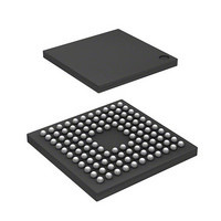
IC H8S/2214 MCU FLASH 112-TFBGA
Manufacturer
Renesas Electronics America
Series
H8® H8S/2200r
Datasheets
1.HS2214ECB62H.pdf
(938 pages)
2.HEWH8E10A.pdf
(19 pages)
3.D12312SVTE25V.pdf
(341 pages)
Specifications of DF2214BQ16V
Core Processor
H8S/2000
Core Size
16-Bit
Speed
16MHz
Connectivity
SCI
Peripherals
DMA, POR, PWM, WDT
Number Of I /o
72
Program Memory Size
128KB (128K x 8)
Program Memory Type
FLASH
Ram Size
12K x 8
Voltage - Supply (vcc/vdd)
2.7 V ~ 3.6 V
Data Converters
D/A 1x8b
Oscillator Type
Internal
Operating Temperature
-20°C ~ 75°C
Package / Case
112-TFBGA
For Use With
HS0005KCU11H - EMULATOR E10A-USB H8S(X),SH2(A)3DK2218 - DEV EVAL KIT H8S/2218
Lead Free Status / RoHS Status
Lead free / RoHS Compliant
Eeprom Size
-
Available stocks
Company
Part Number
Manufacturer
Quantity
Price
Company:

Part Number:
DF2214BQ16V
Manufacturer:
Renesas Electronics America
Quantity:
10 000


Figures
Section 1 Overview
Figure 1.1
Figure 1.2
Figure 1.3
Section 2 CPU
Figure 2.1
Figure 2.2
Figure 2.3
Figure 2.4
Figure 2.5
Figure 2.6
Figure 2.7
Figure 2.8
Figure 2.9
Figure 2.10 General Register Data Formats (1)............................................................................ 31
Figure 2.11 General Register Data Formats (2)............................................................................ 32
Figure 2.12 Memory Data Formats............................................................................................... 33
Figure 2.13 Instruction Formats (Examples) ................................................................................ 47
Figure 2.14 Branch Address Specification in Memory Indirect Mode ......................................... 52
Figure 2.15 Processing States ....................................................................................................... 56
Figure 2.16 State Transitions ........................................................................................................ 57
Figure 2.17 Stack Structure after Exception Handling (Examples) .............................................. 60
Figure 2.18 On-Chip Memory Access Cycle................................................................................ 62
Figure 2.19 Pin States during On-Chip Memory Access.............................................................. 63
Figure 2.20 On-Chip Supporting Module Access Cycle .............................................................. 64
Figure 2.21 Pin States during On-Chip Supporting Module Access............................................. 65
Figure 2.22 Flowchart for Access Methods for Registers that Include Write-Only Bits .............. 69
Section 3 MCU Operating Modes
Figure 3.1
Section 4 Exception Handling
Figure 4.1
Figure 4.2
Reset Sequence (Modes 2 and 3: Not available in the H8S/2214) ............................ 84
H8S/2214 Group Internal Block Diagram................................................................... 5
H8S/2214 Group Pin Arrangement
(TFP-100B, TFP-100BV, TFP-100G, TFP-100GV: Top View)................................. 6
H8S/2214 Group Pin Arrangement
(BP-112, BP-112V, TBP-112A, TBP-112AV: Top View) ......................................... 7
CPU Operating Modes .............................................................................................. 20
Exception Vector Table (Normal Mode)................................................................... 21
Stack Structure in Normal Mode............................................................................... 22
Exception Vector Table (Advanced Mode)............................................................... 23
Stack Structure in Advanced Mode........................................................................... 24
Memory Map............................................................................................................. 25
CPU Registers ........................................................................................................... 26
Usage of General Registers ....................................................................................... 27
Stack .......................................................................................................................... 28
Memory Map in Each Operating Mode in the H8S/2214.......................................... 78
Exception Sources ..................................................................................................... 80
Rev.4.00 Sep. 18, 2008 Page xlv of lx
REJ09B0189-0400
Related parts for DF2214BQ16V
Image
Part Number
Description
Manufacturer
Datasheet
Request
R

Part Number:
Description:
CONN SOCKET 2POS 7.92MM WHITE
Manufacturer:
Hirose Electric Co Ltd
Datasheet:

Part Number:
Description:
CONN SOCKET 4POS 7.92MM WHITE
Manufacturer:
Hirose Electric Co Ltd
Datasheet:

Part Number:
Description:
CONN SOCKET 5POS 7.92MM WHITE
Manufacturer:
Hirose Electric Co Ltd
Datasheet:

Part Number:
Description:
CONN SOCKET 3POS 7.92MM WHITE
Manufacturer:
Hirose Electric Co Ltd
Datasheet:
Part Number:
Description:
CONN SOCKET 5POS 7.92MM WHITE
Manufacturer:
Hirose Electric Co Ltd
Datasheet:

Part Number:
Description:
CONN SOCKET 2POS 7.92MM WHITE
Manufacturer:
Hirose Electric Co Ltd
Datasheet:
Part Number:
Description:
CONN SOCKET 3POS 7.92MM WHITE
Manufacturer:
Hirose Electric Co Ltd
Datasheet:
Part Number:
Description:
CONN SOCKET 4POS 7.92MM WHITE
Manufacturer:
Hirose Electric Co Ltd
Datasheet:

Part Number:
Description:
CONN HEADER 2POS 7.92MM R/A TIN
Manufacturer:
Hirose Electric Co Ltd
Datasheet:

Part Number:
Description:
CONN HEADER 4POS 7.92MM R/A TIN
Manufacturer:
Hirose Electric Co Ltd
Datasheet:

Part Number:
Description:
KIT STARTER FOR M16C/29
Manufacturer:
Renesas Electronics America
Datasheet:

Part Number:
Description:
KIT STARTER FOR R8C/2D
Manufacturer:
Renesas Electronics America
Datasheet:

Part Number:
Description:
R0K33062P STARTER KIT
Manufacturer:
Renesas Electronics America
Datasheet:

Part Number:
Description:
KIT STARTER FOR R8C/23 E8A
Manufacturer:
Renesas Electronics America
Datasheet:

Part Number:
Description:
KIT STARTER FOR R8C/25
Manufacturer:
Renesas Electronics America
Datasheet: