DF2214BQ16V Renesas Electronics America, DF2214BQ16V Datasheet - Page 61
DF2214BQ16V
Manufacturer Part Number
DF2214BQ16V
Description
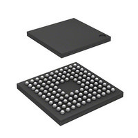
IC H8S/2214 MCU FLASH 112-TFBGA
Manufacturer
Renesas Electronics America
Series
H8® H8S/2200r
Datasheets
1.HS2214ECB62H.pdf
(938 pages)
2.HEWH8E10A.pdf
(19 pages)
3.D12312SVTE25V.pdf
(341 pages)
Specifications of DF2214BQ16V
Core Processor
H8S/2000
Core Size
16-Bit
Speed
16MHz
Connectivity
SCI
Peripherals
DMA, POR, PWM, WDT
Number Of I /o
72
Program Memory Size
128KB (128K x 8)
Program Memory Type
FLASH
Ram Size
12K x 8
Voltage - Supply (vcc/vdd)
2.7 V ~ 3.6 V
Data Converters
D/A 1x8b
Oscillator Type
Internal
Operating Temperature
-20°C ~ 75°C
Package / Case
112-TFBGA
For Use With
HS0005KCU11H - EMULATOR E10A-USB H8S(X),SH2(A)3DK2218 - DEV EVAL KIT H8S/2218
Lead Free Status / RoHS Status
Lead free / RoHS Compliant
Eeprom Size
-
Available stocks
Company
Part Number
Manufacturer
Quantity
Price
Company:

Part Number:
DF2214BQ16V
Manufacturer:
Renesas Electronics America
Quantity:
10 000


Table 15.10 Hardware Protection................................................................................................ 576
Table 15.11 Software Protection ................................................................................................. 577
Table 15.12 Programmer Mode Pin Settings............................................................................... 583
Table 15.13 Settings for Various Operating Modes In Programmer Mode................................. 585
Table 15.14 Programmer Mode Commands................................................................................ 586
Table 15.15 AC Characteristics in Transition to Memory Read Mode ....................................... 586
Table 15.16 AC Characteristics in Transition from Memory Read Mode to Another Mode ...... 587
Table 15.17 AC Characteristics in Memory Read Mode ............................................................ 588
Table 15.18 AC Characteristics in Auto-Program Mode ............................................................ 591
Table 15.19 AC Characteristics in Auto-Erase Mode ................................................................. 592
Table 15.20 AC Characteristics in Status Read Mode ................................................................ 594
Table 15.21 Status Read Mode Return Commands..................................................................... 595
Table 15.22 Status Polling Output Truth Table........................................................................... 595
Table 15.23 Stipulated Transition Times to Command Wait State ............................................. 596
Table 15.24 Flash Memory Operating States .............................................................................. 597
Table 15.25 Registers Present in F-ZTAT Version but Absent in Masked ROM Version ......... 604
Section 16 Clock Pulse Generator
Table 16.1
Table 16.2
Table 16.3
Table 16.4
Table 16.5
Section 17 Power-Down Modes
Table 17.1
Table 17.2
Table 17.3
Table 17.4
Table 17.5
Section 18 Electrical Characteristics
Table 18.1
Table 18.2
Table 18.3
Table 18.4
Table 18.5
Table 18.6
Table 18.7
Table 18.8
Table 18.9
Clock Pulse Generator Register............................................................................... 606
Damping Resistance Value...................................................................................... 609
Crystal Resonator Parameters.................................................................................. 610
External Clock Input Conditions ............................................................................. 612
External Clock Input Conditions when the Duty Adjustment Circuit Is not Used .. 612
LSI Internal States in Each Mode............................................................................ 618
Power-Down Mode Registers.................................................................................. 620
MSTP Bits and Corresponding On-Chip Supporting Modules ............................... 627
Oscillation Stabilization Time Settings ................................................................... 630
φ Pin State in Each Processing Mode ...................................................................... 633
Absolute Maximum Ratings.................................................................................... 635
DC Characteristics (1) ............................................................................................. 637
DC Characteristics (2) ............................................................................................. 639
DC Characteristics (3) ............................................................................................. 640
Permissible Output Currents.................................................................................... 641
Clock Timing........................................................................................................... 642
Control Signal Timing............................................................................................. 644
Bus Timing.............................................................................................................. 646
Timing of On-Chip Supporting Modules ................................................................ 653
Rev.4.00 Sep. 18, 2008 Page lix of lx
REJ09B0189-0400
Related parts for DF2214BQ16V
Image
Part Number
Description
Manufacturer
Datasheet
Request
R

Part Number:
Description:
CONN SOCKET 2POS 7.92MM WHITE
Manufacturer:
Hirose Electric Co Ltd
Datasheet:

Part Number:
Description:
CONN SOCKET 4POS 7.92MM WHITE
Manufacturer:
Hirose Electric Co Ltd
Datasheet:

Part Number:
Description:
CONN SOCKET 5POS 7.92MM WHITE
Manufacturer:
Hirose Electric Co Ltd
Datasheet:

Part Number:
Description:
CONN SOCKET 3POS 7.92MM WHITE
Manufacturer:
Hirose Electric Co Ltd
Datasheet:
Part Number:
Description:
CONN SOCKET 5POS 7.92MM WHITE
Manufacturer:
Hirose Electric Co Ltd
Datasheet:

Part Number:
Description:
CONN SOCKET 2POS 7.92MM WHITE
Manufacturer:
Hirose Electric Co Ltd
Datasheet:
Part Number:
Description:
CONN SOCKET 3POS 7.92MM WHITE
Manufacturer:
Hirose Electric Co Ltd
Datasheet:
Part Number:
Description:
CONN SOCKET 4POS 7.92MM WHITE
Manufacturer:
Hirose Electric Co Ltd
Datasheet:

Part Number:
Description:
CONN HEADER 2POS 7.92MM R/A TIN
Manufacturer:
Hirose Electric Co Ltd
Datasheet:

Part Number:
Description:
CONN HEADER 4POS 7.92MM R/A TIN
Manufacturer:
Hirose Electric Co Ltd
Datasheet:

Part Number:
Description:
KIT STARTER FOR M16C/29
Manufacturer:
Renesas Electronics America
Datasheet:

Part Number:
Description:
KIT STARTER FOR R8C/2D
Manufacturer:
Renesas Electronics America
Datasheet:

Part Number:
Description:
R0K33062P STARTER KIT
Manufacturer:
Renesas Electronics America
Datasheet:

Part Number:
Description:
KIT STARTER FOR R8C/23 E8A
Manufacturer:
Renesas Electronics America
Datasheet:

Part Number:
Description:
KIT STARTER FOR R8C/25
Manufacturer:
Renesas Electronics America
Datasheet: