DF2214BQ16V Renesas Electronics America, DF2214BQ16V Datasheet - Page 59
DF2214BQ16V
Manufacturer Part Number
DF2214BQ16V
Description
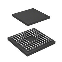
IC H8S/2214 MCU FLASH 112-TFBGA
Manufacturer
Renesas Electronics America
Series
H8® H8S/2200r
Datasheets
1.HS2214ECB62H.pdf
(938 pages)
2.HEWH8E10A.pdf
(19 pages)
3.D12312SVTE25V.pdf
(341 pages)
Specifications of DF2214BQ16V
Core Processor
H8S/2000
Core Size
16-Bit
Speed
16MHz
Connectivity
SCI
Peripherals
DMA, POR, PWM, WDT
Number Of I /o
72
Program Memory Size
128KB (128K x 8)
Program Memory Type
FLASH
Ram Size
12K x 8
Voltage - Supply (vcc/vdd)
2.7 V ~ 3.6 V
Data Converters
D/A 1x8b
Oscillator Type
Internal
Operating Temperature
-20°C ~ 75°C
Package / Case
112-TFBGA
For Use With
HS0005KCU11H - EMULATOR E10A-USB H8S(X),SH2(A)3DK2218 - DEV EVAL KIT H8S/2218
Lead Free Status / RoHS Status
Lead free / RoHS Compliant
Eeprom Size
-
Available stocks
Company
Part Number
Manufacturer
Quantity
Price
Company:

Part Number:
DF2214BQ16V
Manufacturer:
Renesas Electronics America
Quantity:
10 000


Section 9 I/O Ports
Table 9.1
Table 9.2
Table 9.3
Table 9.4
Table 9.5
Table 9.6
Table 9.7
Table 9.8
Table 9.9
Table 9.10
Table 9.11
Table 9.12
Table 9.13
Table 9.14
Table 9.15
Table 9.16
Table 9.17
Table 9.18
Table 9.19
Table 9.20
Table 9.21
Table 9.22
Table 9.23
Table 9.24
Table 9.25
Table 9.26
Section 10 16-Bit Timer Pulse Unit (TPU)
Table 10.1
Table 10.2
Table 10.3
Table 10.4
Table 10.5
Table 10.6
Table 10.7
Table 10.8
Table 10.9
Table 10.10 Up/Down-Count Conditions in Phase Counting Mode 3 ........................................ 414
Table 10.11 Up/Down-Count Conditions in Phase Counting Mode 4 ........................................ 415
H8S/2214 Group Port Functions ............................................................................. 282
Port 1 Registers ....................................................................................................... 286
Port 1 Pin Functions ................................................................................................ 288
Port 3 Registers ....................................................................................................... 297
Port 3 Pin Functions ................................................................................................ 302
Port 4 Registers ....................................................................................................... 304
Port 7 Registers ....................................................................................................... 309
Port 7 Pin Functions ................................................................................................ 312
Port 9 Registers ....................................................................................................... 314
Port A Registers ...................................................................................................... 316
Port A Pin Functions ............................................................................................... 319
MOS Input Pull-Up States (Port A)......................................................................... 321
Port B Registers....................................................................................................... 323
Port B Pin Functions................................................................................................ 325
MOS Input Pull-Up States (Port B)......................................................................... 329
Port C Registers....................................................................................................... 331
MOS Input Pull-Up States (Port C)......................................................................... 336
Port D Registers ...................................................................................................... 338
MOS Input Pull-Up States (Port D)......................................................................... 341
Port E Registers ....................................................................................................... 343
MOS Input Pull-Up States (Port E) ......................................................................... 347
Port F Registers ....................................................................................................... 349
Port F Pin Functions ................................................................................................ 351
Port G Registers ...................................................................................................... 354
Port G Pin Functions ............................................................................................... 356
Handling of Unused Input Pins ............................................................................... 358
TPU Functions......................................................................................................... 361
TPU Pins ................................................................................................................. 364
TPU Registers ......................................................................................................... 365
TPU Clock Sources ................................................................................................. 368
Register Combinations in Buffer Operation............................................................ 401
PWM Output Registers and Output Pins................................................................. 406
Phase Counting Mode Clock Input Pins.................................................................. 411
Up/Down-Count Conditions in Phase Counting Mode 1 ........................................ 412
Up/Down-Count Conditions in Phase Counting Mode 2 ........................................ 413
Rev.4.00 Sep. 18, 2008 Page lvii of lx
REJ09B0189-0400
Related parts for DF2214BQ16V
Image
Part Number
Description
Manufacturer
Datasheet
Request
R

Part Number:
Description:
CONN SOCKET 2POS 7.92MM WHITE
Manufacturer:
Hirose Electric Co Ltd
Datasheet:

Part Number:
Description:
CONN SOCKET 4POS 7.92MM WHITE
Manufacturer:
Hirose Electric Co Ltd
Datasheet:

Part Number:
Description:
CONN SOCKET 5POS 7.92MM WHITE
Manufacturer:
Hirose Electric Co Ltd
Datasheet:

Part Number:
Description:
CONN SOCKET 3POS 7.92MM WHITE
Manufacturer:
Hirose Electric Co Ltd
Datasheet:
Part Number:
Description:
CONN SOCKET 5POS 7.92MM WHITE
Manufacturer:
Hirose Electric Co Ltd
Datasheet:

Part Number:
Description:
CONN SOCKET 2POS 7.92MM WHITE
Manufacturer:
Hirose Electric Co Ltd
Datasheet:
Part Number:
Description:
CONN SOCKET 3POS 7.92MM WHITE
Manufacturer:
Hirose Electric Co Ltd
Datasheet:
Part Number:
Description:
CONN SOCKET 4POS 7.92MM WHITE
Manufacturer:
Hirose Electric Co Ltd
Datasheet:

Part Number:
Description:
CONN HEADER 2POS 7.92MM R/A TIN
Manufacturer:
Hirose Electric Co Ltd
Datasheet:

Part Number:
Description:
CONN HEADER 4POS 7.92MM R/A TIN
Manufacturer:
Hirose Electric Co Ltd
Datasheet:

Part Number:
Description:
KIT STARTER FOR M16C/29
Manufacturer:
Renesas Electronics America
Datasheet:

Part Number:
Description:
KIT STARTER FOR R8C/2D
Manufacturer:
Renesas Electronics America
Datasheet:

Part Number:
Description:
R0K33062P STARTER KIT
Manufacturer:
Renesas Electronics America
Datasheet:

Part Number:
Description:
KIT STARTER FOR R8C/23 E8A
Manufacturer:
Renesas Electronics America
Datasheet:

Part Number:
Description:
KIT STARTER FOR R8C/25
Manufacturer:
Renesas Electronics America
Datasheet: