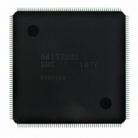
D6417709SF167BV Renesas Electronics America, D6417709SF167BV Datasheet - Page 126

D6417709SF167BV
Manufacturer Part Number
D6417709SF167BV
Description
IC SUPER H MPU ROMLESS 208LQFP
Manufacturer
Renesas Electronics America
Series
SuperH® SH7700r
Datasheet
1.D6417709SBP167BV.pdf
(809 pages)
Specifications of D6417709SF167BV
Core Processor
SH-3
Core Size
32-Bit
Speed
167MHz
Connectivity
EBI/EMI, FIFO, IrDA, SCI, SmartCard
Peripherals
DMA, POR, WDT
Number Of I /o
96
Program Memory Type
ROMless
Ram Size
16K x 8
Voltage - Supply (vcc/vdd)
1.75 V ~ 2.05 V
Data Converters
A/D 8x10b; D/A 2x8b
Oscillator Type
Internal
Operating Temperature
-20°C ~ 75°C
Package / Case
208-LQFP
Lead Free Status / RoHS Status
Lead free / RoHS Compliant
Eeprom Size
-
Program Memory Size
-
Available stocks
Company
Part Number
Manufacturer
Quantity
Price
Company:
Part Number:
D6417709SF167BV
Manufacturer:
Renesas Electronics America
Quantity:
10 000
- Current page: 126 of 809
- Download datasheet (5Mb)
Figure 3.13 shows the MMU exception signals in the data access mode.
3.6
To allow the management of TLB operations by software, the MOV instruction can be used, in the
privileged mode, to read and write TLB contents. The TLB is mapped to the P4 area of the virtual
address space. The TLB address array (VPN, V bit, and ASID) is mapped to H'F2000000 to
H'F2FFFFFF, and the TLB data array (PPN, PR, SZ, CD, S, and H bits) is mapped to H'F3000000
to H'F3FFFFFF. It is also possible to access the V bits in the address array from the data array.
Only longword access is possible, for both the address and data arrays.
3.6.1
The address array is mapped to H'F2000000 to H'F2FFFFFF. To access the address array, the 32-
bit address field (for read/write access) and 32-bit data field (for write access) must be specified.
The address field has the information that selects the entry to be accessed; the data field specifies
the VPN, the V bit, and the ASID to be written to the address array (figure 3.14 (1)).
Rev. 5.00, 09/03, page 80 of 760
NOP
WB
MA
EX
IF
ID
Configuration of Memory-Mapped TLB
Address Array
: Exception source stage
: Stage cancellation for instruction
= Instruction fetch
= Instruction decode
= Instruction execution
= Memory access
= Write back
= No operation
that has begun execution
IF
Figure 3.13 MMU Exception Signals in Data Access
ID
IF
EX
ID
IF
MMU exception handler
MA WB
EX
ID
MA WB
EX
ID
MA WB
EX
ID
MA WB
EX MA
ID
EX
WB
MA WB
IF
NOP
ID
NOP
EX
Handler transition
processing
MA WB
Related parts for D6417709SF167BV
Image
Part Number
Description
Manufacturer
Datasheet
Request
R

Part Number:
Description:
KIT STARTER FOR M16C/29
Manufacturer:
Renesas Electronics America
Datasheet:

Part Number:
Description:
KIT STARTER FOR R8C/2D
Manufacturer:
Renesas Electronics America
Datasheet:

Part Number:
Description:
R0K33062P STARTER KIT
Manufacturer:
Renesas Electronics America
Datasheet:

Part Number:
Description:
KIT STARTER FOR R8C/23 E8A
Manufacturer:
Renesas Electronics America
Datasheet:

Part Number:
Description:
KIT STARTER FOR R8C/25
Manufacturer:
Renesas Electronics America
Datasheet:

Part Number:
Description:
KIT STARTER H8S2456 SHARPE DSPLY
Manufacturer:
Renesas Electronics America
Datasheet:

Part Number:
Description:
KIT STARTER FOR R8C38C
Manufacturer:
Renesas Electronics America
Datasheet:

Part Number:
Description:
KIT STARTER FOR R8C35C
Manufacturer:
Renesas Electronics America
Datasheet:

Part Number:
Description:
KIT STARTER FOR R8CL3AC+LCD APPS
Manufacturer:
Renesas Electronics America
Datasheet:

Part Number:
Description:
KIT STARTER FOR RX610
Manufacturer:
Renesas Electronics America
Datasheet:

Part Number:
Description:
KIT STARTER FOR R32C/118
Manufacturer:
Renesas Electronics America
Datasheet:

Part Number:
Description:
KIT DEV RSK-R8C/26-29
Manufacturer:
Renesas Electronics America
Datasheet:

Part Number:
Description:
KIT STARTER FOR SH7124
Manufacturer:
Renesas Electronics America
Datasheet:

Part Number:
Description:
KIT STARTER FOR H8SX/1622
Manufacturer:
Renesas Electronics America
Datasheet:

Part Number:
Description:
KIT DEV FOR SH7203
Manufacturer:
Renesas Electronics America
Datasheet:


