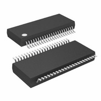
ATMEGA32HVB-8X3 Atmel, ATMEGA32HVB-8X3 Datasheet - Page 206

ATMEGA32HVB-8X3
Manufacturer Part Number
ATMEGA32HVB-8X3
Description
MCU AVR 32KB FLASH 8MHZ 44TSSOP
Manufacturer
Atmel
Series
AVR® ATmegar
Specifications of ATMEGA32HVB-8X3
Core Processor
AVR
Core Size
8-Bit
Speed
8MHz
Connectivity
I²C, SPI
Peripherals
POR, WDT
Number Of I /o
17
Program Memory Size
32KB (16K x 16)
Program Memory Type
FLASH
Eeprom Size
1K x 8
Ram Size
2K x 8
Voltage - Supply (vcc/vdd)
4 V ~ 25 V
Data Converters
A/D 7x12b
Oscillator Type
External
Operating Temperature
-40°C ~ 85°C
Package / Case
44-TSSOP
Processor Series
ATMEGA32x
Core
AVR8
Data Bus Width
8 bit
Data Ram Size
2 KB
Interface Type
SPI, TWI
Maximum Clock Frequency
8 MHz
Number Of Programmable I/os
17
Number Of Timers
2
Maximum Operating Temperature
+ 85 C
Mounting Style
SMD/SMT
Development Tools By Supplier
ATAVRDRAGON, ATSTK500, ATSTK600, ATAVRISP2, ATAVRONEKIT, ATAVRSB200
Minimum Operating Temperature
- 40 C
On-chip Adc
12 bit, 7 Channel
Package
44TSSOP
Device Core
AVR
Family Name
ATmega
Maximum Speed
8 MHz
Operating Supply Voltage
5|9|12|15|18|24 V
For Use With
ATSTK524 - KIT STARTER ATMEGA32M1/MEGA32C1ATSTK600 - DEV KIT FOR AVR/AVR32ATAVRDRAGON - KIT DRAGON 32KB FLASH MEM AVRATSTK500 - PROGRAMMER AVR STARTER KIT
Lead Free Status / RoHS Status
Lead free / RoHS Compliant
Available stocks
Company
Part Number
Manufacturer
Quantity
Price
Company:
Part Number:
ATMEGA32HVB-8X3
Manufacturer:
Atmel
Quantity:
408
- Current page: 206 of 275
- Download datasheet (7Mb)
29.9
29.9.1
8042B–AVR–06/10
Register Description
SPMCSR – Store Program Memory Control and Status Register
The Store Program Memory Control and Status Register contains the control bits needed to con-
trol the Boot Loader operations.
• Bit 7 – SPMIE: SPM Interrupt Enable
When the SPMIE bit is written to one, and the I-bit in the Status Register is set (one), the SPM
ready interrupt will be enabled. The SPM ready Interrupt will be executed as long as the SPMEN
bit in the SPMCSR Register is cleared.
• Bit 6 – RWWSB: Read-While-Write Section Busy
When a Self-Programming (Page Erase or Page Write) operation to the RWW section is initi-
ated, the RWWSB will be set (one) by hardware. When the RWWSB bit is set, the RWW section
cannot be accessed. The RWWSB bit will be cleared if the RWWSRE bit is written to one after a
Self-Programming operation is completed. Alternatively the RWWSB bit will automatically be
cleared if a page load operation is initiated.
• Bit 5 - SIGRD: Signature Row Read
If this bit is written to one at the same time as SPMEN, the next LPM instruction within three
clock cycles will read a byte from the signature row into the destination register.
the Signature Row from Software” on page 199
An SPM instruction within four cycles after SIGRD and SPMEN are set will have no effect. This
operation is reserved for future use and should not be used.
• Bit 4 – RWWSRE: Read-While-Write Section Read Enable
When programming (Page Erase or Page Write) to the RWW section, the RWW section is
blocked for reading (the RWWSB will be set by hardware). To re-enable the RWW section, the
user software must wait until the programming is completed (SPMEN will be cleared). Then, if
the RWWSRE bit is written to one at the same time as SPMEN, the next SPM instruction within
four clock cycles re-enables the RWW section. The RWW section cannot be re-enabled while
the Flash is busy with a Page Erase or a Page Write (SPMEN is set). If the RWWSRE bit is writ-
ten while the Flash is being loaded, the Flash load operation will abort and the data loaded will
be lost.
• Bit 3 – LBSET: Lock Bit Set
If this bit is written to one at the same time as SPMEN, the next SPM instruction within four clock
cycles sets Lock bits, according to the data in R0. The data in R1 and the address in the Z-
pointer are ignored. The LBSET bit will automatically be cleared upon completion of the Lock bit
set, or after six cycles if no SPM instruction is executed within four clock cycles.
An LPM instruction within three cycles after LBSET and SPMEN are set in the SPMCSR Regis-
ter, will read either the Lock bits or the Fuse bits (depending on Z0 in the Z-pointer) into the
destination register. See
Bit
0x37 (0x57)
Read/Write
Initial Value
SPMIE
R/W
7
0
RWWSB
R
6
0
”Reading the Fuse and Lock Bits” on page 224
SIGRD
R/W
5
0
RWWSRE
R/W
4
0
for details.
LBSET
ATmega16HVB/32HVB
R/W
3
0
PGWRT
R/W
2
0
PGERS
R/W
1
0
for details.
SPMEN
R/W
0
0
See”Reading
SPMCSR
206
Related parts for ATMEGA32HVB-8X3
Image
Part Number
Description
Manufacturer
Datasheet
Request
R

Part Number:
Description:
Manufacturer:
Atmel Corporation
Datasheet:

Part Number:
Description:
Manufacturer:
ATMEL Corporation
Datasheet:

Part Number:
Description:
IC AVR MCU 32K 16MHZ 5V 44-QFN
Manufacturer:
Atmel
Datasheet:

Part Number:
Description:
IC AVR MCU 32K 16MHZ 5V 40DIP
Manufacturer:
Atmel
Datasheet:

Part Number:
Description:
IC AVR MCU 32K 16MHZ 5V 44TQFP
Manufacturer:
Atmel
Datasheet:

Part Number:
Description:
IC AVR MCU 32K 16MHZ IND 40-DIP
Manufacturer:
Atmel
Datasheet:

Part Number:
Description:
IC AVR MCU 32K 16MHZ IND 44-TQFP
Manufacturer:
Atmel
Datasheet:

Part Number:
Description:
MCU AVR 32KB FLASH 16MHZ 44TQFP
Manufacturer:
Atmel
Datasheet:

Part Number:
Description:
MCU AVR 32KB FLASH 16MHZ 44QFN
Manufacturer:
Atmel
Datasheet:

Part Number:
Description:
MCU AVR 32K FLASH 16MHZ 44-TQFP
Manufacturer:
Atmel
Datasheet:

Part Number:
Description:
IC AVR MCU 32K 16MHZ COM 40-DIP
Manufacturer:
Atmel
Datasheet:

Part Number:
Description:
IC AVR MCU 32K 16MHZ COM 44-QFN
Manufacturer:
Atmel
Datasheet:

Part Number:
Description:
IC AVR MCU 32K 16MHZ COM 44-TQFP
Manufacturer:
Atmel
Datasheet:


