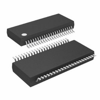
ATMEGA32HVB-8X3 Atmel, ATMEGA32HVB-8X3 Datasheet - Page 39

ATMEGA32HVB-8X3
Manufacturer Part Number
ATMEGA32HVB-8X3
Description
MCU AVR 32KB FLASH 8MHZ 44TSSOP
Manufacturer
Atmel
Series
AVR® ATmegar
Specifications of ATMEGA32HVB-8X3
Core Processor
AVR
Core Size
8-Bit
Speed
8MHz
Connectivity
I²C, SPI
Peripherals
POR, WDT
Number Of I /o
17
Program Memory Size
32KB (16K x 16)
Program Memory Type
FLASH
Eeprom Size
1K x 8
Ram Size
2K x 8
Voltage - Supply (vcc/vdd)
4 V ~ 25 V
Data Converters
A/D 7x12b
Oscillator Type
External
Operating Temperature
-40°C ~ 85°C
Package / Case
44-TSSOP
Processor Series
ATMEGA32x
Core
AVR8
Data Bus Width
8 bit
Data Ram Size
2 KB
Interface Type
SPI, TWI
Maximum Clock Frequency
8 MHz
Number Of Programmable I/os
17
Number Of Timers
2
Maximum Operating Temperature
+ 85 C
Mounting Style
SMD/SMT
Development Tools By Supplier
ATAVRDRAGON, ATSTK500, ATSTK600, ATAVRISP2, ATAVRONEKIT, ATAVRSB200
Minimum Operating Temperature
- 40 C
On-chip Adc
12 bit, 7 Channel
Package
44TSSOP
Device Core
AVR
Family Name
ATmega
Maximum Speed
8 MHz
Operating Supply Voltage
5|9|12|15|18|24 V
For Use With
ATSTK524 - KIT STARTER ATMEGA32M1/MEGA32C1ATSTK600 - DEV KIT FOR AVR/AVR32ATAVRDRAGON - KIT DRAGON 32KB FLASH MEM AVRATSTK500 - PROGRAMMER AVR STARTER KIT
Lead Free Status / RoHS Status
Lead free / RoHS Compliant
Available stocks
Company
Part Number
Manufacturer
Quantity
Price
Company:
Part Number:
ATMEGA32HVB-8X3
Manufacturer:
Atmel
Quantity:
408
- Current page: 39 of 275
- Download datasheet (7Mb)
10.7.3
10.7.4
10.7.5
10.7.6
10.7.7
10.8
10.8.1
8042B–AVR–06/10
Register Description
On-chip Debug System
Battery Protection
Voltage ADC
Coulomb Counter
Bandgap Voltage Reference
SMCR – Sleep Mode Control Register
some cases, the input logic is needed for detecting wake-up conditions, and it will then be
enabled. Refer to the section
which pins are enabled. If the input buffer is enabled and the input signal is left floating or have
an analog signal level close to V
For analog input pins, the digital input buffer should be disabled at all times. An analog signal
level close to V
input buffers can be disabled by writing to the Digital Input Disable Register. Refer to
Digital Input Disable Register 0” on page 122
A programmed DWEN Fuse enables some parts of the clock system to be running in all sleep
modes. This will increase the power consumption while in sleep. Thus, the DWEN Fuse should
be disabled when debugWire is not used.
If one of the Battery Protection features is not needed by the application, this feature should be
disabled, see “BPCR – Battery Protection Control Register” on page 141. The current consump-
tion in the Battery Protection circuitry is only significant in Power-save mode. Disabling both
FETs will automatically disable the Battery Protection module in order to save power. The band-
gap reference should always be enabled whenever Battery Protection is enabled.
If enabled, the V-ADC will consume power independent of sleep mode. To save power, the V-
ADC should be disabled when not used, and before entering Power-save sleep mode. See
”Voltage ADC – 7-channel General Purpose 12-bit Sigma-Delta ADC” on page 117
V-ADC operation.
If enabled, the CC-ADC will consume power independent of sleep mode. To save power, the
CC-ADC should be disabled when not used, or set in Regular Current detection mode. See
”Coulomb Counter – Dedicated Fuel Gauging Sigma-delta ADC” on page 108
ADC operation.
If enabled, the Bandgap reference will consume power independent of sleep mode. To save
power, the Bandgap reference should be disabled when not used as reference for the Voltage
ADC, the Coloumb Counter or Battery Protection. See
Sensor” on page 123
The Sleep Mode Control Register contains control bits for power management.
Bit
0x33 (0x53)
Read/Write
Initial Value
REG
R
7
–
0
/2 on an input pin can cause significant current even in active mode. Digital
for details.
R
6
–
0
”Digital Input Enable and Sleep Modes” on page 71
REG
R
5
–
0
/2, the input buffer will use excessive power.
R
4
–
0
for details.
SM2
ATmega16HVB/32HVB
R/W
3
0
”Voltage Reference and Temperature
SM1
R/W
2
0
SM0
R/W
1
0
for details on CC-
R/W
SE
0
0
for details on
for details on
”DIDR0 –
SMCR
39
Related parts for ATMEGA32HVB-8X3
Image
Part Number
Description
Manufacturer
Datasheet
Request
R

Part Number:
Description:
Manufacturer:
Atmel Corporation
Datasheet:

Part Number:
Description:
Manufacturer:
ATMEL Corporation
Datasheet:

Part Number:
Description:
IC AVR MCU 32K 16MHZ 5V 44-QFN
Manufacturer:
Atmel
Datasheet:

Part Number:
Description:
IC AVR MCU 32K 16MHZ 5V 40DIP
Manufacturer:
Atmel
Datasheet:

Part Number:
Description:
IC AVR MCU 32K 16MHZ 5V 44TQFP
Manufacturer:
Atmel
Datasheet:

Part Number:
Description:
IC AVR MCU 32K 16MHZ IND 40-DIP
Manufacturer:
Atmel
Datasheet:

Part Number:
Description:
IC AVR MCU 32K 16MHZ IND 44-TQFP
Manufacturer:
Atmel
Datasheet:

Part Number:
Description:
MCU AVR 32KB FLASH 16MHZ 44TQFP
Manufacturer:
Atmel
Datasheet:

Part Number:
Description:
MCU AVR 32KB FLASH 16MHZ 44QFN
Manufacturer:
Atmel
Datasheet:

Part Number:
Description:
MCU AVR 32K FLASH 16MHZ 44-TQFP
Manufacturer:
Atmel
Datasheet:

Part Number:
Description:
IC AVR MCU 32K 16MHZ COM 40-DIP
Manufacturer:
Atmel
Datasheet:

Part Number:
Description:
IC AVR MCU 32K 16MHZ COM 44-QFN
Manufacturer:
Atmel
Datasheet:

Part Number:
Description:
IC AVR MCU 32K 16MHZ COM 44-TQFP
Manufacturer:
Atmel
Datasheet:


