ATMEGA32HVB-8X3 Atmel, ATMEGA32HVB-8X3 Datasheet - Page 58
ATMEGA32HVB-8X3
Manufacturer Part Number
ATMEGA32HVB-8X3
Description
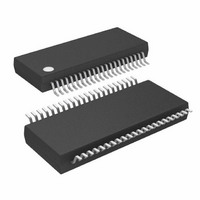
MCU AVR 32KB FLASH 8MHZ 44TSSOP
Manufacturer
Atmel
Series
AVR® ATmegar
Specifications of ATMEGA32HVB-8X3
Core Processor
AVR
Core Size
8-Bit
Speed
8MHz
Connectivity
I²C, SPI
Peripherals
POR, WDT
Number Of I /o
17
Program Memory Size
32KB (16K x 16)
Program Memory Type
FLASH
Eeprom Size
1K x 8
Ram Size
2K x 8
Voltage - Supply (vcc/vdd)
4 V ~ 25 V
Data Converters
A/D 7x12b
Oscillator Type
External
Operating Temperature
-40°C ~ 85°C
Package / Case
44-TSSOP
Processor Series
ATMEGA32x
Core
AVR8
Data Bus Width
8 bit
Data Ram Size
2 KB
Interface Type
SPI, TWI
Maximum Clock Frequency
8 MHz
Number Of Programmable I/os
17
Number Of Timers
2
Maximum Operating Temperature
+ 85 C
Mounting Style
SMD/SMT
Development Tools By Supplier
ATAVRDRAGON, ATSTK500, ATSTK600, ATAVRISP2, ATAVRONEKIT, ATAVRSB200
Minimum Operating Temperature
- 40 C
On-chip Adc
12 bit, 7 Channel
Package
44TSSOP
Device Core
AVR
Family Name
ATmega
Maximum Speed
8 MHz
Operating Supply Voltage
5|9|12|15|18|24 V
For Use With
ATSTK524 - KIT STARTER ATMEGA32M1/MEGA32C1ATSTK600 - DEV KIT FOR AVR/AVR32ATAVRDRAGON - KIT DRAGON 32KB FLASH MEM AVRATSTK500 - PROGRAMMER AVR STARTER KIT
Lead Free Status / RoHS Status
Lead free / RoHS Compliant
Available stocks
Company
Part Number
Manufacturer
Quantity
Price
Company:

Part Number:
ATMEGA32HVB-8X3
Manufacturer:
Atmel
Quantity:
408


13. External Interrupts
13.1
13.2
13.2.1
8042B–AVR–06/10
Overview
Register Description
EICRA – External Interrupt Control Register A
The External Interrupts are triggered by the INT3:0 pin or any of the PCINT11:0 pins. Observe
that, if enabled, the interrupts will trigger even if the INT3:0 or PCINT11:0 pins are configured as
outputs. This feature provides a way of generating a software interrupt.
The External Interrupts can be triggered by a falling or rising edge or a low level. This is set up
as indicated in the specification for the
58. When the external interrupt is enabled and is configured as level triggered, the interrupt will
trigger as long as the pin is held low. Interrupts are detected asynchronously. This implies that
these interrupts can be used for waking the part also from sleep modes other than Idle mode.
The I/O clock is halted in all sleep modes except Idle mode.
The Pin change interrupt PCI1 will trigger if any enabled PCINT11:4 pin toggles and Pin change
interrupts PCI0 will trigger if any enabled PCINT3:0 pin toggles. PCMSK1 and PCMSK0 Regis-
ters control which pins contribute to the pin change interrupts. Pin change interrupts on
PCINT11:0 are detected asynchronously. This implies that these interrupts can be used for wak-
ing the part also from sleep modes other than Idle mode.
Note that if a level triggered interrupt is used for wake-up from Power-save, the required level
must be held long enough for the MCU to complete the wake-up to trigger the level interrupt. If
the level disappears before the end of the Start-up Time, the MCU will still wake up, but no inter-
rupt will be generated. The start-up time is defined by the SUT fuses as described in
Systems and their Distribution” on page
• Bits 7:0 – ISCn: External Interrupt Sense Control Bits
The External Interrupts 3:0 are activated by the external pins INT3:0 if the SREG I-flag and the
corresponding interrupt mask in the EIMSK is set. The level and edges on the external pins that
activate the interrupts are defined in
asynchronously. Pulses on INT3:0 pins wider than the minimum pulse width given in
11 on page 235
interrupt. If low level interrupt is selected, the low level must be held until the completion of the
currently executing instruction to generate an interrupt. If enabled, a level triggered interrupt will
generate an interrupt request as long as the pin is held low. When changing the ISCn bit, an
interrupt can occur. Therefore, it is recommended to first disable INTn by clearing its Interrupt
Enable bit in the EIMSK Register. Then, the ISCn bit can be changed. Finally, the INTn interrupt
flag should be cleared by writing a logical one to its Interrupt Flag bit (INTFn) in the EIFR Regis-
ter before the interrupt is re-enabled.
Bit
(0x69)
Read/Write
Initial Value
ISC31
R/W
will generate an interrupt. Shorter pulses are not guaranteed to generate an
7
0
ISC30
R/W
6
0
ISC21
R/W
5
0
Table 13-1 on page
”EICRA – External Interrupt Control Register A” on page
25.
ISC20
R/W
4
0
ISC11
ATmega16HVB/32HVB
R/W
3
0
59. Edges on INT3..INT0 are registered
ISC10
R/W
2
0
ISC01
R/W
1
0
ISC00
R/W
0
0
Table 32-
EICRA
”Clock
58
Related parts for ATMEGA32HVB-8X3
Image
Part Number
Description
Manufacturer
Datasheet
Request
R

Part Number:
Description:
Manufacturer:
Atmel Corporation
Datasheet:
Part Number:
Description:
Manufacturer:
ATMEL Corporation
Datasheet:

Part Number:
Description:
IC AVR MCU 32K 16MHZ 5V 44-QFN
Manufacturer:
Atmel
Datasheet:

Part Number:
Description:
IC AVR MCU 32K 16MHZ 5V 40DIP
Manufacturer:
Atmel
Datasheet:

Part Number:
Description:
IC AVR MCU 32K 16MHZ 5V 44TQFP
Manufacturer:
Atmel
Datasheet:
Part Number:
Description:
IC AVR MCU 32K 16MHZ IND 40-DIP
Manufacturer:
Atmel
Datasheet:
Part Number:
Description:
IC AVR MCU 32K 16MHZ IND 44-TQFP
Manufacturer:
Atmel
Datasheet:

Part Number:
Description:
MCU AVR 32KB FLASH 16MHZ 44TQFP
Manufacturer:
Atmel
Datasheet:
Part Number:
Description:
MCU AVR 32KB FLASH 16MHZ 44QFN
Manufacturer:
Atmel
Datasheet:
Part Number:
Description:
MCU AVR 32K FLASH 16MHZ 44-TQFP
Manufacturer:
Atmel
Datasheet:
Part Number:
Description:
IC AVR MCU 32K 16MHZ COM 40-DIP
Manufacturer:
Atmel
Datasheet:
Part Number:
Description:
IC AVR MCU 32K 16MHZ COM 44-QFN
Manufacturer:
Atmel
Datasheet:
Part Number:
Description:
IC AVR MCU 32K 16MHZ COM 44-TQFP
Manufacturer:
Atmel
Datasheet: