R5F21324ANSP#U1 Renesas Electronics America, R5F21324ANSP#U1 Datasheet - Page 14
R5F21324ANSP#U1
Manufacturer Part Number
R5F21324ANSP#U1
Description
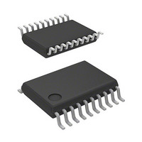
MCU 1KB FLASH 16K ROM 20-LSSOP
Manufacturer
Renesas Electronics America
Series
R8C/3x/32Ar
Datasheet
1.R5F21322ANSPU1.pdf
(629 pages)
Specifications of R5F21324ANSP#U1
Core Processor
R8C
Core Size
16/32-Bit
Speed
20MHz
Connectivity
I²C, LIN, SIO, SSU, UART/USART
Peripherals
POR, PWM, Voltage Detect, WDT
Number Of I /o
15
Program Memory Size
16KB (16K x 8)
Program Memory Type
FLASH
Ram Size
1.5K x 8
Voltage - Supply (vcc/vdd)
1.8 V ~ 5.5 V
Data Converters
A/D 4x10b
Oscillator Type
Internal
Operating Temperature
-20°C ~ 85°C
Package / Case
20-LSSOP
Lead Free Status / RoHS Status
Lead free / RoHS Compliant
Eeprom Size
-
Available stocks
Company
Part Number
Manufacturer
Quantity
Price


13.
14.
15.
12.3
12.4
12.5
13.1
13.2
13.3
14.1
14.2
14.3
15.1
15.2
15.3
12.5.1
13.2.1
13.2.2
13.3.1
14.2.1
14.2.2
14.2.3
14.2.4
14.2.5
14.2.6
14.2.7
14.3.1
14.3.2
14.3.3
15.2.1
15.2.2
15.2.3
15.2.4
15.2.5
15.2.6
15.2.7
15.2.8
15.3.1
15.3.2
15.3.3
15.3.4
15.3.5
15.3.6
15.3.7
15.3.8
15.3.9
Option Function Select Area ....................................................................................................... 152
Watchdog Timer .......................................................................................................................... 156
DTC ............................................................................................................................................ 165
Forced Erase Function ........................................................................................................................... 150
Standard Serial II/O Mode Disabled Function ...................................................................................... 150
Notes on ID Code Areas ........................................................................................................................ 151
Overview ............................................................................................................................................... 152
Registers ................................................................................................................................................ 153
Notes on Option Function Select Area .................................................................................................. 155
Overview ............................................................................................................................................... 156
Registers ................................................................................................................................................ 158
Overview ............................................................................................................................................... 165
Registers ................................................................................................................................................ 166
Function Description ............................................................................................................................. 171
Functional Description ......................................................................................................................... 162
Setting Example of ID Code Areas ................................................................................................... 151
Option Function Select Register (OFS) ............................................................................................ 153
Option Function Select Register 2 (OFS2) ....................................................................................... 154
Setting Example of Option Function Select Area ............................................................................. 155
Processor Mode Register 1 (PM1) .................................................................................................... 158
Watchdog Timer Reset Register (WDTR) ........................................................................................ 158
Watchdog Timer Start Register (WDTS) ......................................................................................... 158
Watchdog Timer Control Register (WDTC) .................................................................................... 159
Count Source Protection Mode Register (CSPR) ............................................................................. 159
Option Function Select Register (OFS) ............................................................................................ 160
Option Function Select Register 2 (OFS2) ....................................................................................... 161
Common Items for Multiple Modes ................................................................................................. 162
Count Source Protection Mode Disabled .......................................................................................... 163
Count Source Protection Mode Enabled ........................................................................................... 164
DTC Control Register j (DTCCRj) (j = 0 to 23) ............................................................................... 167
DTC Block Size Register j (DTBLSj) (j = 0 to 23) .......................................................................... 167
DTC Transfer Count Register j (DTCCTj) (j = 0 to 23) ................................................................... 168
DTC Transfer Count Reload Register j (DTRLDj) (j = 0 to 23) ...................................................... 168
DTC Source Address Register j (DTSARj) (j = 0 to 23) .................................................................. 168
DTC Destination Register j (DTDARj) (j = 0 to 23) ........................................................................ 168
DTC Activation Enable Register i (DTCENi) (i = 0 to 3, 5, 6) ........................................................ 169
DTC Activation Control Register (DTCTL) .................................................................................... 170
Overview ........................................................................................................................................... 171
Activation Sources ............................................................................................................................ 171
Control Data Allocation and DTC Vector Table .............................................................................. 173
Normal Mode .................................................................................................................................... 178
Repeat Mode ..................................................................................................................................... 179
Chain Transfers ................................................................................................................................. 180
Interrupt Sources ............................................................................................................................... 180
Operation Timings ............................................................................................................................ 181
Number of DTC Execution Cycles ................................................................................................... 182
A - 5
Related parts for R5F21324ANSP#U1
Image
Part Number
Description
Manufacturer
Datasheet
Request
R

Part Number:
Description:
KIT STARTER FOR M16C/29
Manufacturer:
Renesas Electronics America
Datasheet:

Part Number:
Description:
KIT STARTER FOR R8C/2D
Manufacturer:
Renesas Electronics America
Datasheet:

Part Number:
Description:
R0K33062P STARTER KIT
Manufacturer:
Renesas Electronics America
Datasheet:

Part Number:
Description:
KIT STARTER FOR R8C/23 E8A
Manufacturer:
Renesas Electronics America
Datasheet:

Part Number:
Description:
KIT STARTER FOR R8C/25
Manufacturer:
Renesas Electronics America
Datasheet:

Part Number:
Description:
KIT STARTER H8S2456 SHARPE DSPLY
Manufacturer:
Renesas Electronics America
Datasheet:

Part Number:
Description:
KIT STARTER FOR R8C38C
Manufacturer:
Renesas Electronics America
Datasheet:

Part Number:
Description:
KIT STARTER FOR R8C35C
Manufacturer:
Renesas Electronics America
Datasheet:

Part Number:
Description:
KIT STARTER FOR R8CL3AC+LCD APPS
Manufacturer:
Renesas Electronics America
Datasheet:
Part Number:
Description:
KIT STARTER FOR RX610
Manufacturer:
Renesas Electronics America
Datasheet:

Part Number:
Description:
KIT STARTER FOR R32C/118
Manufacturer:
Renesas Electronics America
Datasheet:

Part Number:
Description:
KIT DEV RSK-R8C/26-29
Manufacturer:
Renesas Electronics America
Datasheet:

Part Number:
Description:
KIT STARTER FOR SH7124
Manufacturer:
Renesas Electronics America
Datasheet:

Part Number:
Description:
KIT STARTER FOR H8SX/1622
Manufacturer:
Renesas Electronics America
Datasheet:

Part Number:
Description:
KIT DEV FOR SH7203
Manufacturer:
Renesas Electronics America
Datasheet: