R5F21324ANSP#U1 Renesas Electronics America, R5F21324ANSP#U1 Datasheet - Page 622
R5F21324ANSP#U1
Manufacturer Part Number
R5F21324ANSP#U1
Description
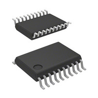
MCU 1KB FLASH 16K ROM 20-LSSOP
Manufacturer
Renesas Electronics America
Series
R8C/3x/32Ar
Datasheet
1.R5F21322ANSPU1.pdf
(629 pages)
Specifications of R5F21324ANSP#U1
Core Processor
R8C
Core Size
16/32-Bit
Speed
20MHz
Connectivity
I²C, LIN, SIO, SSU, UART/USART
Peripherals
POR, PWM, Voltage Detect, WDT
Number Of I /o
15
Program Memory Size
16KB (16K x 8)
Program Memory Type
FLASH
Ram Size
1.5K x 8
Voltage - Supply (vcc/vdd)
1.8 V ~ 5.5 V
Data Converters
A/D 4x10b
Oscillator Type
Internal
Operating Temperature
-20°C ~ 85°C
Package / Case
20-LSSOP
Lead Free Status / RoHS Status
Lead free / RoHS Compliant
Eeprom Size
-
Available stocks
Company
Part Number
Manufacturer
Quantity
Price


RENESAS TECHNICAL UPDATE
2.1.2 Timer RA Register Setting
2.1.3 Timer RC Register Setting
2.1.4 Timer RD Register Setting (only for the R8C/35A Group, R8C/36A Group, R8C/38A Group, and R8C/3JA
2.1.1.3 High-Speed On-Chip Oscillator Cotrol Registers 1 to 7 (FRA1 to FRA7)
2.1.2.1 High-Speed On-Chip Oscillator Control Register 0 (FRA0)
2.1.3.1 Timer RC Control Register 1 (TRCCR1)
2.1.3.2 High-Speed On-Chip Oscillator Control Register 0 (FRA0)
2.1.4.1 Timer RD Control Register 0, 1 (TRDCR0, TRDCR1)
2.1.4.2 High-Speed On-Chip Oscillator Control Register 0 (FRA0)
(1) Do not set bits TCK2 to TCK0 to 110b (fOCO40M selected for the timer RD count source) [refer to Figure
(1) Do not set the register related to the high-speed on-chip oscillator division select (FRA2) or registers
(1) Do not set the FRA01 bit to 1 (high-speed on-chip oscillator selected for the fOCO clock) [refer to
(1) Do not set bits TCK2 to TCK0 to 110b (fOCO40M selected for the timer RC count source) [refer to
(2) Do not set bits TCK2 to TCK0 to 111b (fOCO-F selected for the timer RC count source) [refer to Figure
(1) Do not set the FRA03 bit to 1 (fOCO-F divided by 128 selected for the fOCO128 clock) [refer to Figure
∗ The R8C/32A Group, R8C/33A Group, and R8C/3GA Group are not equipped with timer RD.
(2) Do not set bits TCK2 to TCK0 to 111b (fOCO-F selected for the timer RD count source) [refer to Figure
(1) Do not set the FRA03 bit to 1 (fOCO-F divided by 128 selected for the fOCO128 clock) [refer to Figure
Group
related to the frequency adjustment (FRA1 and FRA3 to FRA7) .
Figure 2.1]. The high-speed on-chip oscillator clock cannot be selected for the timer RA count source.
Figure 2.3].
2.3].
2.1]. For the timer RC input-capture function, fOCO-F divided by 128 cannot be selected for the
input-capture trigger input of the TRCGRA register.
2.4].
2.4].
2.1]. For the timer RD input-capture function, fOCO-F divided by 128 cannot be selected for the
input-capture trigger input of the TRDGRA0 register.
*
)
TN-R8C-A001B/E
Date: Sep.24.2009
Page 2 of 9
Related parts for R5F21324ANSP#U1
Image
Part Number
Description
Manufacturer
Datasheet
Request
R

Part Number:
Description:
KIT STARTER FOR M16C/29
Manufacturer:
Renesas Electronics America
Datasheet:

Part Number:
Description:
KIT STARTER FOR R8C/2D
Manufacturer:
Renesas Electronics America
Datasheet:

Part Number:
Description:
R0K33062P STARTER KIT
Manufacturer:
Renesas Electronics America
Datasheet:

Part Number:
Description:
KIT STARTER FOR R8C/23 E8A
Manufacturer:
Renesas Electronics America
Datasheet:

Part Number:
Description:
KIT STARTER FOR R8C/25
Manufacturer:
Renesas Electronics America
Datasheet:

Part Number:
Description:
KIT STARTER H8S2456 SHARPE DSPLY
Manufacturer:
Renesas Electronics America
Datasheet:

Part Number:
Description:
KIT STARTER FOR R8C38C
Manufacturer:
Renesas Electronics America
Datasheet:

Part Number:
Description:
KIT STARTER FOR R8C35C
Manufacturer:
Renesas Electronics America
Datasheet:

Part Number:
Description:
KIT STARTER FOR R8CL3AC+LCD APPS
Manufacturer:
Renesas Electronics America
Datasheet:
Part Number:
Description:
KIT STARTER FOR RX610
Manufacturer:
Renesas Electronics America
Datasheet:

Part Number:
Description:
KIT STARTER FOR R32C/118
Manufacturer:
Renesas Electronics America
Datasheet:

Part Number:
Description:
KIT DEV RSK-R8C/26-29
Manufacturer:
Renesas Electronics America
Datasheet:

Part Number:
Description:
KIT STARTER FOR SH7124
Manufacturer:
Renesas Electronics America
Datasheet:

Part Number:
Description:
KIT STARTER FOR H8SX/1622
Manufacturer:
Renesas Electronics America
Datasheet:

Part Number:
Description:
KIT DEV FOR SH7203
Manufacturer:
Renesas Electronics America
Datasheet: