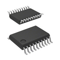
R5F21324ANSP#U1 Renesas Electronics America, R5F21324ANSP#U1 Datasheet - Page 526

R5F21324ANSP#U1
Manufacturer Part Number
R5F21324ANSP#U1
Description
MCU 1KB FLASH 16K ROM 20-LSSOP
Manufacturer
Renesas Electronics America
Series
R8C/3x/32Ar
Datasheet
1.R5F21322ANSPU1.pdf
(629 pages)
Specifications of R5F21324ANSP#U1
Core Processor
R8C
Core Size
16/32-Bit
Speed
20MHz
Connectivity
I²C, LIN, SIO, SSU, UART/USART
Peripherals
POR, PWM, Voltage Detect, WDT
Number Of I /o
15
Program Memory Size
16KB (16K x 8)
Program Memory Type
FLASH
Ram Size
1.5K x 8
Voltage - Supply (vcc/vdd)
1.8 V ~ 5.5 V
Data Converters
A/D 4x10b
Oscillator Type
Internal
Operating Temperature
-20°C ~ 85°C
Package / Case
20-LSSOP
Lead Free Status / RoHS Status
Lead free / RoHS Compliant
Eeprom Size
-
Available stocks
Company
Part Number
Manufacturer
Quantity
Price
- Current page: 526 of 629
- Download datasheet (7Mb)
Under development
R8C/32A Group
REJ09B0458-0020 Rev.0.20
Page 496 of 583
30.4.3
Notes:
1. To set the FMR13 bit to 1, first write 0 and then 1 immediately. Do not generate an interrupt between writing 0
2. To set this bit to 0, first write 1 and then 0 immediately. Do not generate an interrupt between writing 1 and
FMR13 Bit (Lock Bit Disable Select Bit)
After Reset
Bit
b0
b1
b2
b3
b4
b5
b6
b7
Address 01B5h
[Conditions for setting to 0]
The FMR13 bit is set to 0 when one of the following conditions is met.
[Condition for setting to 1]
Set to 1 by a program.
and writing 1.
writing 0.
When the FMR13 bit is set to 1 (lock bit disabled), the lock bit is disabled. When the FMR13 bit is set to 0, the
lock bit is enabled. Refer to 30.4.10 Data Protect Function for the details of the lock bit.
The FMR13 bit enables the lock bit function only and the lock bit data does not change. However, when a block
erase command is executed while the FMR13 bit is set to 1, the lock bit data set to 0 (locked) changes to 1 (not
locked) after erasure completes.
•
•
•
•
•
•
•
Symbol
Completion of the program command
Completion of the erase command
Generation of a command error
Transition to erase-suspend
If the FMR01 bit in the FMR0 register is set to 0 (CPU rewrite mode disabled).
If the FMSTP bit in the FMR0 register is set to 1 (flash memory stops).
If the CMDRST bit in the FMR0 register is set to 1 (erasure/writing stopped).
Symbol
FMR10 Nothing is assigned. If necessary, set to 0. When read, the content is 0.
FMR11
FMR12
FMR13 Lock bit disable select bit
FMR14 Data flash block A rewrite
FMR15 Data flash block B rewrite
FMR16 Data flash block C rewrite
FMR17 Data flash block D rewrite
Bit
Flash Memory Control Register 1 (FMR1)
FMR17
Preliminary specification
Specifications in this manual are tentative and subject to change.
b7
0
disable bit
disable bit
disable bit
disable bit
FMR16
b6
0
(2)
(2)
(2)
(2)
Bit Name
Nov 05, 2008
FMR15
b5
0
(1)
FMR14
b4
0
0: Lock bit enabled
1: Lock bit disabled
0: Rewrite enabled (software command acceptable)
1: Rewrite disabled (software command not acceptable,
0: Rewrite enabled (software command acceptable)
1: Rewrite disabled (software command not acceptable,
0: Rewrite enabled (software command acceptable)
1: Rewrite disabled (software command not acceptable,
0: Rewrite enabled (software command acceptable)
1: Rewrite disabled (software command not acceptable,
no error occurred)
no error occurred)
no error occurred)
no error occurred)
FMR13
b3
0
FMR12
b2
0
Function
FMR11
b1
0
FMR10
b0
0
30. Flash Memory
R/W
R/W
R/W
R/W
R/W
R/W
—
—
—
Related parts for R5F21324ANSP#U1
Image
Part Number
Description
Manufacturer
Datasheet
Request
R

Part Number:
Description:
KIT STARTER FOR M16C/29
Manufacturer:
Renesas Electronics America
Datasheet:

Part Number:
Description:
KIT STARTER FOR R8C/2D
Manufacturer:
Renesas Electronics America
Datasheet:

Part Number:
Description:
R0K33062P STARTER KIT
Manufacturer:
Renesas Electronics America
Datasheet:

Part Number:
Description:
KIT STARTER FOR R8C/23 E8A
Manufacturer:
Renesas Electronics America
Datasheet:

Part Number:
Description:
KIT STARTER FOR R8C/25
Manufacturer:
Renesas Electronics America
Datasheet:

Part Number:
Description:
KIT STARTER H8S2456 SHARPE DSPLY
Manufacturer:
Renesas Electronics America
Datasheet:

Part Number:
Description:
KIT STARTER FOR R8C38C
Manufacturer:
Renesas Electronics America
Datasheet:

Part Number:
Description:
KIT STARTER FOR R8C35C
Manufacturer:
Renesas Electronics America
Datasheet:

Part Number:
Description:
KIT STARTER FOR R8CL3AC+LCD APPS
Manufacturer:
Renesas Electronics America
Datasheet:

Part Number:
Description:
KIT STARTER FOR RX610
Manufacturer:
Renesas Electronics America
Datasheet:

Part Number:
Description:
KIT STARTER FOR R32C/118
Manufacturer:
Renesas Electronics America
Datasheet:

Part Number:
Description:
KIT DEV RSK-R8C/26-29
Manufacturer:
Renesas Electronics America
Datasheet:

Part Number:
Description:
KIT STARTER FOR SH7124
Manufacturer:
Renesas Electronics America
Datasheet:

Part Number:
Description:
KIT STARTER FOR H8SX/1622
Manufacturer:
Renesas Electronics America
Datasheet:

Part Number:
Description:
KIT DEV FOR SH7203
Manufacturer:
Renesas Electronics America
Datasheet:


