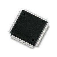
MC9S12DT256MPVE Freescale Semiconductor, MC9S12DT256MPVE Datasheet - Page 1274

MC9S12DT256MPVE
Manufacturer Part Number
MC9S12DT256MPVE
Description
IC MCU 256K FLASH 25MHZ 112-LQFP
Manufacturer
Freescale Semiconductor
Series
HCS12r
Datasheet
1.S912XDG128F2MAL.pdf
(1348 pages)
Specifications of MC9S12DT256MPVE
Core Processor
HCS12
Core Size
16-Bit
Speed
25MHz
Connectivity
CAN, I²C, SCI, SPI
Peripherals
PWM, WDT
Number Of I /o
91
Program Memory Size
256KB (256K x 8)
Program Memory Type
FLASH
Eeprom Size
4K x 8
Ram Size
12K x 8
Voltage - Supply (vcc/vdd)
2.35 V ~ 5.25 V
Data Converters
A/D 8x10b
Oscillator Type
Internal
Operating Temperature
-40°C ~ 125°C
Package / Case
112-LQFP
Processor Series
S12D
Core
HCS12
Data Bus Width
16 bit
Data Ram Size
12 KB
Interface Type
CAN/I2C/SCI/SPI
Maximum Clock Frequency
25 MHz
Number Of Programmable I/os
91
Number Of Timers
1
Operating Supply Voltage
5 V to 2.5 V
Maximum Operating Temperature
+ 125 C
Mounting Style
SMD/SMT
3rd Party Development Tools
EWHCS12
Development Tools By Supplier
M68KIT912DP256
Minimum Operating Temperature
- 40 C
On-chip Adc
2 (8-ch x 10-bit)
No. Of I/o's
91
Eeprom Memory Size
4KB
Ram Memory Size
12KB
Cpu Speed
25MHz
No. Of Timers
1
No. Of Pwm Channels
8
Digital Ic Case Style
LQFP
Rohs Compliant
Yes
Lead Free Status / RoHS Status
Lead free / RoHS Compliant
Available stocks
Company
Part Number
Manufacturer
Quantity
Price
Company:
Part Number:
MC9S12DT256MPVE
Manufacturer:
Freescale Semiconductor
Quantity:
10 000
- Current page: 1274 of 1348
- Download datasheet (8Mb)
Appendix A Electrical Characteristics
In
In Master Mode the allowed maximum f
SPI Section) derates with increasing f
A.7.2
In
1276
f
SCK
Table A-26
Num
Figure A-9
10
11
12
13
1
1
2
3
4
5
6
9
/f
1/4
1/2
bus
C
D
D
D
D
D
D
D
D
D
D
D
D
Slave Mode
the timing diagram for slave mode with transmission format CPHA = 0 is depicted.
the timing characteristics for master mode are listed.
Figure A-8.
SCK frequency
SCK period
Enable lead time
Enable lag time
Clock (SCK) high or low time
Data setup time (inputs)
Data hold time (inputs)
Data valid after SCK edge
Data valid after SS fall (CPHA = 0)
Data hold time (outputs)
Rise and fall time inputs
Rise and fall time outputs
5
10
Derating of maximum f
Table A-26. SPI Master Mode Timing Characteristics
Characteristic
15
MC9S12XDP512 Data Sheet, Rev. 2.21
20
bus.
SCK
25
to f
bus
SCK
Symbol
30
ratio (= minimum Baud Rate Divisor, pls. see
t
t
t
f
t
wsck
t
t
lead
vsck
t
t
t
t
sck
sck
t
vss
lag
su
ho
rfo
hi
rfi
to f
bus
35
1/2048
Min
ratio in Master Mode
—
—
—
—
—
—
—
2
8
8
0
40
Typ
1/2
1/2
1/2
—
—
—
—
—
—
—
—
—
f
bus
Freescale Semiconductor
[MHz]
2048
Max
1 2
15
15
—
—
—
—
—
—
8
8
Unit
f
t
t
t
t
bus
bus
ns
ns
ns
ns
ns
ns
ns
sck
sck
sck
Related parts for MC9S12DT256MPVE
Image
Part Number
Description
Manufacturer
Datasheet
Request
R
Part Number:
Description:
Manufacturer:
Freescale Semiconductor, Inc
Datasheet:
Part Number:
Description:
Manufacturer:
Freescale Semiconductor, Inc
Datasheet:
Part Number:
Description:
Manufacturer:
Freescale Semiconductor, Inc
Datasheet:
Part Number:
Description:
Manufacturer:
Freescale Semiconductor, Inc
Datasheet:
Part Number:
Description:
Manufacturer:
Freescale Semiconductor, Inc
Datasheet:
Part Number:
Description:
Manufacturer:
Freescale Semiconductor, Inc
Datasheet:
Part Number:
Description:
Manufacturer:
Freescale Semiconductor, Inc
Datasheet:
Part Number:
Description:
Manufacturer:
Freescale Semiconductor, Inc
Datasheet:
Part Number:
Description:
Manufacturer:
Freescale Semiconductor, Inc
Datasheet:
Part Number:
Description:
Manufacturer:
Freescale Semiconductor, Inc
Datasheet:
Part Number:
Description:
Manufacturer:
Freescale Semiconductor, Inc
Datasheet:
Part Number:
Description:
Manufacturer:
Freescale Semiconductor, Inc
Datasheet:
Part Number:
Description:
Manufacturer:
Freescale Semiconductor, Inc
Datasheet:
Part Number:
Description:
Manufacturer:
Freescale Semiconductor, Inc
Datasheet:
Part Number:
Description:
Manufacturer:
Freescale Semiconductor, Inc
Datasheet:


