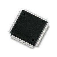
MC9S12DT256MPVE Freescale Semiconductor, MC9S12DT256MPVE Datasheet - Page 946

MC9S12DT256MPVE
Manufacturer Part Number
MC9S12DT256MPVE
Description
IC MCU 256K FLASH 25MHZ 112-LQFP
Manufacturer
Freescale Semiconductor
Series
HCS12r
Datasheet
1.S912XDG128F2MAL.pdf
(1348 pages)
Specifications of MC9S12DT256MPVE
Core Processor
HCS12
Core Size
16-Bit
Speed
25MHz
Connectivity
CAN, I²C, SCI, SPI
Peripherals
PWM, WDT
Number Of I /o
91
Program Memory Size
256KB (256K x 8)
Program Memory Type
FLASH
Eeprom Size
4K x 8
Ram Size
12K x 8
Voltage - Supply (vcc/vdd)
2.35 V ~ 5.25 V
Data Converters
A/D 8x10b
Oscillator Type
Internal
Operating Temperature
-40°C ~ 125°C
Package / Case
112-LQFP
Processor Series
S12D
Core
HCS12
Data Bus Width
16 bit
Data Ram Size
12 KB
Interface Type
CAN/I2C/SCI/SPI
Maximum Clock Frequency
25 MHz
Number Of Programmable I/os
91
Number Of Timers
1
Operating Supply Voltage
5 V to 2.5 V
Maximum Operating Temperature
+ 125 C
Mounting Style
SMD/SMT
3rd Party Development Tools
EWHCS12
Development Tools By Supplier
M68KIT912DP256
Minimum Operating Temperature
- 40 C
On-chip Adc
2 (8-ch x 10-bit)
No. Of I/o's
91
Eeprom Memory Size
4KB
Ram Memory Size
12KB
Cpu Speed
25MHz
No. Of Timers
1
No. Of Pwm Channels
8
Digital Ic Case Style
LQFP
Rohs Compliant
Yes
Lead Free Status / RoHS Status
Lead free / RoHS Compliant
Available stocks
Company
Part Number
Manufacturer
Quantity
Price
Company:
Part Number:
MC9S12DT256MPVE
Manufacturer:
Freescale Semiconductor
Quantity:
10 000
- Current page: 946 of 1348
- Download datasheet (8Mb)
Chapter 23 DQ256 Port Integration Module (S12XDQ256PIMV2)
23.0.5.47 Port H Input Register (PTIH)
Read: Anytime.
Write: Never, writes to this register have no effect.
This register always reads back the buffered state of the associated pins. This can also be used to detect
overload or short circuit conditions on output pins.
23.0.5.48 Port H Data Direction Register (DDRH)
Read: Anytime.
Write: Anytime.
This register configures each port H pin as either input or output.
If the associated routed SPI module is enabled this register has no effect on the pins.
The SCI forces the I/O state to be an output for each port line associated with an enabled output ( TXD4).
It also forces the I/O state to be an input for each port line associated with an enabled input ( RXD4). In
those cases the data direction bits will not change.
If a SPI module is enabled, the SPI determines the pin direction. Refer to SPI section for details.
The DDRH bits revert to controlling the I/O direction of a pin when the associated peripheral modules are
disabled.
948
Reset
Reset
1. These registers are reset to zero. Two bus clock cycles after reset release the register values are updated with the
W
associated pin values.
W
R
R
1
DDRH7
PTIH7
—
0
7
7
= Unimplemented or Reserved
DDRH6
PTIH6
—
0
6
6
Figure 23-50. Port H Data Direction Register (DDRH)
Figure 23-49. Port H Input Register (PTIH)
DDRH5
MC9S12XDP512 Data Sheet, Rev. 2.21
PTIH5
—
0
5
5
DDRH4
PTIH4
—
0
4
4
DDRH3
PTIH3
—
0
3
3
DDRH2
PTIH2
—
0
2
2
DDRH1
Freescale Semiconductor
PTIH1
—
0
1
1
DDRH0
PTIH0
—
0
0
0
Related parts for MC9S12DT256MPVE
Image
Part Number
Description
Manufacturer
Datasheet
Request
R
Part Number:
Description:
Manufacturer:
Freescale Semiconductor, Inc
Datasheet:
Part Number:
Description:
Manufacturer:
Freescale Semiconductor, Inc
Datasheet:
Part Number:
Description:
Manufacturer:
Freescale Semiconductor, Inc
Datasheet:
Part Number:
Description:
Manufacturer:
Freescale Semiconductor, Inc
Datasheet:
Part Number:
Description:
Manufacturer:
Freescale Semiconductor, Inc
Datasheet:
Part Number:
Description:
Manufacturer:
Freescale Semiconductor, Inc
Datasheet:
Part Number:
Description:
Manufacturer:
Freescale Semiconductor, Inc
Datasheet:
Part Number:
Description:
Manufacturer:
Freescale Semiconductor, Inc
Datasheet:
Part Number:
Description:
Manufacturer:
Freescale Semiconductor, Inc
Datasheet:
Part Number:
Description:
Manufacturer:
Freescale Semiconductor, Inc
Datasheet:
Part Number:
Description:
Manufacturer:
Freescale Semiconductor, Inc
Datasheet:
Part Number:
Description:
Manufacturer:
Freescale Semiconductor, Inc
Datasheet:
Part Number:
Description:
Manufacturer:
Freescale Semiconductor, Inc
Datasheet:
Part Number:
Description:
Manufacturer:
Freescale Semiconductor, Inc
Datasheet:
Part Number:
Description:
Manufacturer:
Freescale Semiconductor, Inc
Datasheet:


