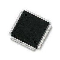
MC9S12DT256MPVE Freescale Semiconductor, MC9S12DT256MPVE Datasheet - Page 358

MC9S12DT256MPVE
Manufacturer Part Number
MC9S12DT256MPVE
Description
IC MCU 256K FLASH 25MHZ 112-LQFP
Manufacturer
Freescale Semiconductor
Series
HCS12r
Datasheet
1.S912XDG128F2MAL.pdf
(1348 pages)
Specifications of MC9S12DT256MPVE
Core Processor
HCS12
Core Size
16-Bit
Speed
25MHz
Connectivity
CAN, I²C, SCI, SPI
Peripherals
PWM, WDT
Number Of I /o
91
Program Memory Size
256KB (256K x 8)
Program Memory Type
FLASH
Eeprom Size
4K x 8
Ram Size
12K x 8
Voltage - Supply (vcc/vdd)
2.35 V ~ 5.25 V
Data Converters
A/D 8x10b
Oscillator Type
Internal
Operating Temperature
-40°C ~ 125°C
Package / Case
112-LQFP
Processor Series
S12D
Core
HCS12
Data Bus Width
16 bit
Data Ram Size
12 KB
Interface Type
CAN/I2C/SCI/SPI
Maximum Clock Frequency
25 MHz
Number Of Programmable I/os
91
Number Of Timers
1
Operating Supply Voltage
5 V to 2.5 V
Maximum Operating Temperature
+ 125 C
Mounting Style
SMD/SMT
3rd Party Development Tools
EWHCS12
Development Tools By Supplier
M68KIT912DP256
Minimum Operating Temperature
- 40 C
On-chip Adc
2 (8-ch x 10-bit)
No. Of I/o's
91
Eeprom Memory Size
4KB
Ram Memory Size
12KB
Cpu Speed
25MHz
No. Of Timers
1
No. Of Pwm Channels
8
Digital Ic Case Style
LQFP
Rohs Compliant
Yes
Lead Free Status / RoHS Status
Lead free / RoHS Compliant
Available stocks
Company
Part Number
Manufacturer
Quantity
Price
Company:
Part Number:
MC9S12DT256MPVE
Manufacturer:
Freescale Semiconductor
Quantity:
10 000
- Current page: 358 of 1348
- Download datasheet (8Mb)
Chapter 7 Enhanced Capture Timer (S12ECT16B8CV2)
7.4.1.1.3
There are four delay counters in this module associated with IC channels 0–3. The use of this feature is
explained in the diagram and notes below.
In
358
Figure 7-72
2. IC Queue Mode (LATQ = 0)
1. Input pulses with a duration of (DLY_CNT – 1) cycles or shorter are rejected.
2. Input pulses with a duration between (DLY_CNT – 1) and DLY_CNT cycles may be rejected or
3. Input pulses with a duration between (DLY_CNT – 1) and DLY_CNT cycles may be rejected or
4. Input pulses with a duration of DLY_CNT or longer are accepted.
If the corresponding NOVWx bit of the ICOVW register is set, the capture register or its holding
register cannot be written by an event unless they are empty (see
This will prevent the captured value from being overwritten until it is read or latched in the holding
register.
The main timer value is memorized in the IC register by a valid input pin transition (see
and
If the corresponding NOVWx bit of the ICOVW register is cleared, with a new occurrence of a
capture, the value of the IC register will be transferred to its holding register and the IC register
memorizes the new timer value.
If the corresponding NOVWx bit of the ICOVW register is set, the capture register or its holding
register cannot be written by an event unless they are empty (see
In queue mode, reads of the holding register will latch the corresponding pulse accumulator value
to its holding register.
accepted, depending on their relative alignment with the sample points.
accepted, depending on their relative alignment with the sample points.
Figure
BUS CLOCK
Delayed IC Channels
a delay counter value of 256 bus cycles is considered.
INPUT ON
INPUT ON
INPUT ON
INPUT ON
DLY_CNT
CH0–3
CH0–3
CH0–3
CH0–3
7-68).
Figure 7-72. Channel Input Validity with Delay Counter Feature
0
MC9S12XDP512 Data Sheet, Rev. 2.21
1
2
255.5 Cycles
255.5 Cycles
255 Cycles
256 Cycles
3
253
254
255
Section 7.4.1.1, “IC
Section 7.4.1.1, “IC
256
Accepted
Rejected
Accepted
Rejected
Freescale Semiconductor
Channels”).
Figure 7-67
Channels”).
Related parts for MC9S12DT256MPVE
Image
Part Number
Description
Manufacturer
Datasheet
Request
R
Part Number:
Description:
Manufacturer:
Freescale Semiconductor, Inc
Datasheet:
Part Number:
Description:
Manufacturer:
Freescale Semiconductor, Inc
Datasheet:
Part Number:
Description:
Manufacturer:
Freescale Semiconductor, Inc
Datasheet:
Part Number:
Description:
Manufacturer:
Freescale Semiconductor, Inc
Datasheet:
Part Number:
Description:
Manufacturer:
Freescale Semiconductor, Inc
Datasheet:
Part Number:
Description:
Manufacturer:
Freescale Semiconductor, Inc
Datasheet:
Part Number:
Description:
Manufacturer:
Freescale Semiconductor, Inc
Datasheet:
Part Number:
Description:
Manufacturer:
Freescale Semiconductor, Inc
Datasheet:
Part Number:
Description:
Manufacturer:
Freescale Semiconductor, Inc
Datasheet:
Part Number:
Description:
Manufacturer:
Freescale Semiconductor, Inc
Datasheet:
Part Number:
Description:
Manufacturer:
Freescale Semiconductor, Inc
Datasheet:
Part Number:
Description:
Manufacturer:
Freescale Semiconductor, Inc
Datasheet:
Part Number:
Description:
Manufacturer:
Freescale Semiconductor, Inc
Datasheet:
Part Number:
Description:
Manufacturer:
Freescale Semiconductor, Inc
Datasheet:
Part Number:
Description:
Manufacturer:
Freescale Semiconductor, Inc
Datasheet:


