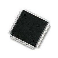
MC9S12DT256MPVE Freescale Semiconductor, MC9S12DT256MPVE Datasheet - Page 148

MC9S12DT256MPVE
Manufacturer Part Number
MC9S12DT256MPVE
Description
IC MCU 256K FLASH 25MHZ 112-LQFP
Manufacturer
Freescale Semiconductor
Series
HCS12r
Datasheet
1.S912XDG128F2MAL.pdf
(1348 pages)
Specifications of MC9S12DT256MPVE
Core Processor
HCS12
Core Size
16-Bit
Speed
25MHz
Connectivity
CAN, I²C, SCI, SPI
Peripherals
PWM, WDT
Number Of I /o
91
Program Memory Size
256KB (256K x 8)
Program Memory Type
FLASH
Eeprom Size
4K x 8
Ram Size
12K x 8
Voltage - Supply (vcc/vdd)
2.35 V ~ 5.25 V
Data Converters
A/D 8x10b
Oscillator Type
Internal
Operating Temperature
-40°C ~ 125°C
Package / Case
112-LQFP
Processor Series
S12D
Core
HCS12
Data Bus Width
16 bit
Data Ram Size
12 KB
Interface Type
CAN/I2C/SCI/SPI
Maximum Clock Frequency
25 MHz
Number Of Programmable I/os
91
Number Of Timers
1
Operating Supply Voltage
5 V to 2.5 V
Maximum Operating Temperature
+ 125 C
Mounting Style
SMD/SMT
3rd Party Development Tools
EWHCS12
Development Tools By Supplier
M68KIT912DP256
Minimum Operating Temperature
- 40 C
On-chip Adc
2 (8-ch x 10-bit)
No. Of I/o's
91
Eeprom Memory Size
4KB
Ram Memory Size
12KB
Cpu Speed
25MHz
No. Of Timers
1
No. Of Pwm Channels
8
Digital Ic Case Style
LQFP
Rohs Compliant
Yes
Lead Free Status / RoHS Status
Lead free / RoHS Compliant
Available stocks
Company
Part Number
Manufacturer
Quantity
Price
Company:
Part Number:
MC9S12DT256MPVE
Manufacturer:
Freescale Semiconductor
Quantity:
10 000
- Current page: 148 of 1348
- Download datasheet (8Mb)
Chapter 4 Analog-to-Digital Converter (ATD10B16CV4) Block Description
4.3.2.12
Read: Anytime
Write: anytime
4.3.2.13
Read: Anytime
Write: Anytime
148
IEN[15:8]
Reset
Reset
IEN[7:0]
Field
Field
7:0
7:0
W
W
R
R
IEN15
IEN7
ATD Input Enable Register 0 (ATDDIEN0)
ATD Input Enable Register 1 (ATDDIEN1)
0
0
7
7
ATD Digital Input Enable on Channel Bits — This bit controls the digital input buffer from the analog input
pin (ANx) to PTADx data register.
0 Disable digital input buffer to PTADx
1 Enable digital input buffer to PTADx.
Note: Setting this bit will enable the corresponding digital input buffer continuously. If this bit is set while
simultaneously using it as an analog port, there is potentially increased power consumption because the
digital input buffer maybe in the linear region.
simultaneously using it as an analog port, there is potentially increased power consumption because the
digital input buffer maybe in the linear region.
IEN14
IEN6
0
0
6
6
Figure 4-14. ATD Input Enable Register 0 (ATDDIEN0)
Figure 4-15. ATD Input Enable Register 1 (ATDDIEN1)
Table 4-23. ATDDIEN0 Field Descriptions
Table 4-24. ATDDIEN1 Field Descriptions
MC9S12XDP512 Data Sheet, Rev. 2.21
IEN13
IEN5
0
0
5
5
IEN12
IEN4
0
0
4
4
Description
Description
IEN11
IEN3
0
0
3
3
IEN10
IEN2
0
0
2
2
Freescale Semiconductor
IEN9
IEN1
0
0
1
1
IEN8
IEN0
0
0
0
0
Related parts for MC9S12DT256MPVE
Image
Part Number
Description
Manufacturer
Datasheet
Request
R
Part Number:
Description:
Manufacturer:
Freescale Semiconductor, Inc
Datasheet:
Part Number:
Description:
Manufacturer:
Freescale Semiconductor, Inc
Datasheet:
Part Number:
Description:
Manufacturer:
Freescale Semiconductor, Inc
Datasheet:
Part Number:
Description:
Manufacturer:
Freescale Semiconductor, Inc
Datasheet:
Part Number:
Description:
Manufacturer:
Freescale Semiconductor, Inc
Datasheet:
Part Number:
Description:
Manufacturer:
Freescale Semiconductor, Inc
Datasheet:
Part Number:
Description:
Manufacturer:
Freescale Semiconductor, Inc
Datasheet:
Part Number:
Description:
Manufacturer:
Freescale Semiconductor, Inc
Datasheet:
Part Number:
Description:
Manufacturer:
Freescale Semiconductor, Inc
Datasheet:
Part Number:
Description:
Manufacturer:
Freescale Semiconductor, Inc
Datasheet:
Part Number:
Description:
Manufacturer:
Freescale Semiconductor, Inc
Datasheet:
Part Number:
Description:
Manufacturer:
Freescale Semiconductor, Inc
Datasheet:
Part Number:
Description:
Manufacturer:
Freescale Semiconductor, Inc
Datasheet:
Part Number:
Description:
Manufacturer:
Freescale Semiconductor, Inc
Datasheet:
Part Number:
Description:
Manufacturer:
Freescale Semiconductor, Inc
Datasheet:


