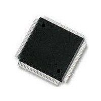
MC9S12DT256MPVE Freescale Semiconductor, MC9S12DT256MPVE Datasheet - Page 798

MC9S12DT256MPVE
Manufacturer Part Number
MC9S12DT256MPVE
Description
IC MCU 256K FLASH 25MHZ 112-LQFP
Manufacturer
Freescale Semiconductor
Series
HCS12r
Datasheet
1.S912XDG128F2MAL.pdf
(1348 pages)
Specifications of MC9S12DT256MPVE
Core Processor
HCS12
Core Size
16-Bit
Speed
25MHz
Connectivity
CAN, I²C, SCI, SPI
Peripherals
PWM, WDT
Number Of I /o
91
Program Memory Size
256KB (256K x 8)
Program Memory Type
FLASH
Eeprom Size
4K x 8
Ram Size
12K x 8
Voltage - Supply (vcc/vdd)
2.35 V ~ 5.25 V
Data Converters
A/D 8x10b
Oscillator Type
Internal
Operating Temperature
-40°C ~ 125°C
Package / Case
112-LQFP
Processor Series
S12D
Core
HCS12
Data Bus Width
16 bit
Data Ram Size
12 KB
Interface Type
CAN/I2C/SCI/SPI
Maximum Clock Frequency
25 MHz
Number Of Programmable I/os
91
Number Of Timers
1
Operating Supply Voltage
5 V to 2.5 V
Maximum Operating Temperature
+ 125 C
Mounting Style
SMD/SMT
3rd Party Development Tools
EWHCS12
Development Tools By Supplier
M68KIT912DP256
Minimum Operating Temperature
- 40 C
On-chip Adc
2 (8-ch x 10-bit)
No. Of I/o's
91
Eeprom Memory Size
4KB
Ram Memory Size
12KB
Cpu Speed
25MHz
No. Of Timers
1
No. Of Pwm Channels
8
Digital Ic Case Style
LQFP
Rohs Compliant
Yes
Lead Free Status / RoHS Status
Lead free / RoHS Compliant
Available stocks
Company
Part Number
Manufacturer
Quantity
Price
Company:
Part Number:
MC9S12DT256MPVE
Manufacturer:
Freescale Semiconductor
Quantity:
10 000
- Current page: 798 of 1348
- Download datasheet (8Mb)
Chapter 21 External Bus Interface (S12XEBIV2)
21.4.5.2
In emulation modes and special test mode, the external signals LSTRB, R/W, and ADDR0 indicate the
access type (read/write), data size and alignment of an external bus access. Misaligned accesses to the
internal RAM and misaligned XGATE PRR accesses in emulation modes are the only type of access that
are able to produce LSTRB = ADDR0 = 1. This is summarized in
800
Word write of data on DATA[15:0] at an even and even+1 address
Byte write of data on DATA[7:0] at an odd address
Byte write of data on DATA[15:8] at an even address
Word read of data on DATA[15:0] at an even and even+1 address
Byte read of data on DATA[7:0] at an odd address
Byte read of data on DATA[15:8] at an even address
Indicates No Access
Unimplemented
Word write of data on DATA[15:0] at an even and even+1
address
Byte write of data on DATA[7:0] at an odd address
Byte write of data on DATA[15:8] at an even address
Word write at an odd and odd+1 internal RAM address
(misaligned — only in emulation modes)
Word read of data on DATA[15:0] at an even and even+1
address
Byte read of data on DATA[7:0] at an odd address
Byte read of data on DATA[15:8] at an even address
Word read at an odd and odd+1 internal RAM address
(misaligned - only in emulation modes)
Emulation Modes and Special Test Mode
Table 21-18. Access in Emulation Modes and Special Test Mode
Access
Access
Table 21-17. Access in Normal Expanded Mode
MC9S12XDP512 Data Sheet, Rev. 2.21
R/W LSTRB ADDR0
0
0
0
0
1
1
1
1
RE WE UDS LDS
1
1
1
0
0
0
1
1
1
0
0
1
1
0
0
1
1
0
0
0
1
1
1
1
1
1
Table
0
1
0
1
0
1
0
1
0
1
0
0
1
0
1
1
0
Out
Out
Out data(odd+1) Out
0
0
1
0
0
1
1
0
1
I/O
21-18.
In
In
In
In
In
DATA[15:8]
Out data(even) Out data(odd)
Out data(even)
I/O data(addr) I/O data(addr)
In
In
In
In
In
In
In
data(odd+1)
data(addr)
data(even)
data(even)
data(even)
data(odd)
DATA[15:8]
data(even)
data(even)
x
x
Freescale Semiconductor
x
x
x
x
x
Out
Out
I/O
In
In
In
In
In
Out data(odd)
In
In
In
In
In
In
In
DATA[7:0]
DATA[7:0]
data(even+1)
data(addr)
data(odd)
data(odd)
data(odd)
data(odd)
data(odd)
data(odd)
data(odd)
x
x
x
x
x
x
x
Related parts for MC9S12DT256MPVE
Image
Part Number
Description
Manufacturer
Datasheet
Request
R
Part Number:
Description:
Manufacturer:
Freescale Semiconductor, Inc
Datasheet:
Part Number:
Description:
Manufacturer:
Freescale Semiconductor, Inc
Datasheet:
Part Number:
Description:
Manufacturer:
Freescale Semiconductor, Inc
Datasheet:
Part Number:
Description:
Manufacturer:
Freescale Semiconductor, Inc
Datasheet:
Part Number:
Description:
Manufacturer:
Freescale Semiconductor, Inc
Datasheet:
Part Number:
Description:
Manufacturer:
Freescale Semiconductor, Inc
Datasheet:
Part Number:
Description:
Manufacturer:
Freescale Semiconductor, Inc
Datasheet:
Part Number:
Description:
Manufacturer:
Freescale Semiconductor, Inc
Datasheet:
Part Number:
Description:
Manufacturer:
Freescale Semiconductor, Inc
Datasheet:
Part Number:
Description:
Manufacturer:
Freescale Semiconductor, Inc
Datasheet:
Part Number:
Description:
Manufacturer:
Freescale Semiconductor, Inc
Datasheet:
Part Number:
Description:
Manufacturer:
Freescale Semiconductor, Inc
Datasheet:
Part Number:
Description:
Manufacturer:
Freescale Semiconductor, Inc
Datasheet:
Part Number:
Description:
Manufacturer:
Freescale Semiconductor, Inc
Datasheet:
Part Number:
Description:
Manufacturer:
Freescale Semiconductor, Inc
Datasheet:


