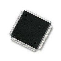
MC9S12DT256MPVE Freescale Semiconductor, MC9S12DT256MPVE Datasheet - Page 169

MC9S12DT256MPVE
Manufacturer Part Number
MC9S12DT256MPVE
Description
IC MCU 256K FLASH 25MHZ 112-LQFP
Manufacturer
Freescale Semiconductor
Series
HCS12r
Datasheet
1.S912XDG128F2MAL.pdf
(1348 pages)
Specifications of MC9S12DT256MPVE
Core Processor
HCS12
Core Size
16-Bit
Speed
25MHz
Connectivity
CAN, I²C, SCI, SPI
Peripherals
PWM, WDT
Number Of I /o
91
Program Memory Size
256KB (256K x 8)
Program Memory Type
FLASH
Eeprom Size
4K x 8
Ram Size
12K x 8
Voltage - Supply (vcc/vdd)
2.35 V ~ 5.25 V
Data Converters
A/D 8x10b
Oscillator Type
Internal
Operating Temperature
-40°C ~ 125°C
Package / Case
112-LQFP
Processor Series
S12D
Core
HCS12
Data Bus Width
16 bit
Data Ram Size
12 KB
Interface Type
CAN/I2C/SCI/SPI
Maximum Clock Frequency
25 MHz
Number Of Programmable I/os
91
Number Of Timers
1
Operating Supply Voltage
5 V to 2.5 V
Maximum Operating Temperature
+ 125 C
Mounting Style
SMD/SMT
3rd Party Development Tools
EWHCS12
Development Tools By Supplier
M68KIT912DP256
Minimum Operating Temperature
- 40 C
On-chip Adc
2 (8-ch x 10-bit)
No. Of I/o's
91
Eeprom Memory Size
4KB
Ram Memory Size
12KB
Cpu Speed
25MHz
No. Of Timers
1
No. Of Pwm Channels
8
Digital Ic Case Style
LQFP
Rohs Compliant
Yes
Lead Free Status / RoHS Status
Lead free / RoHS Compliant
Available stocks
Company
Part Number
Manufacturer
Quantity
Price
Company:
Part Number:
MC9S12DT256MPVE
Manufacturer:
Freescale Semiconductor
Quantity:
10 000
- Current page: 169 of 1348
- Download datasheet (8Mb)
5.3.2.4
This register controls the conversion sequence length, FIFO for results registers and behavior in freeze
mode. Writes to this register will abort current conversion sequence but will not start a new sequence.
Read: Anytime
Write: Anytime
Freescale Semiconductor
S8C, S4C,
S2C, S1C
Reset
ASCIE
ASCIF
Field
Field
6–3
1
0
W
R
Conversion Sequence Length — These bits control the number of conversions per sequence.
all combinations. At reset, S4C is set to 1 (sequence length is 4). This is to maintain software continuity to HC12
Family.
ATD Control Register 3 (ATDCTL3)
0
0
7
ATD Sequence Complete Interrupt Enable
0 ATD Sequence Complete interrupt requests are disabled.
1 ATD Interrupt will be requested whenever ASCIF = 1 is set.
ATD Sequence Complete Interrupt Flag — If ASCIE = 1 the ASCIF flag equals the SCF flag (see
Section 5.3.2.7, “ATD Status Register 0
0 No ATD interrupt occurred
1 ATD sequence complete interrupt pending
= Unimplemented or Reserved
S8C
0
6
ETRIGLE
Table 5-5. ATDCTL2 Field Descriptions (continued)
Figure 5-6. ATD Control Register 3 (ATDCTL3)
0
0
1
1
Table 5-6. External Trigger Configurations
Table 5-7. ATDCTL3 Field Descriptions
MC9S12XDP512 Data Sheet, Rev. 2.21
S4C
0
5
ETRIGP
0
1
0
1
(ATDSTAT0)”), else ASCIF reads zero. Writes have no effect.
S2C
0
4
Description
Description
External Trigger Sensitivity
Chapter 5 Analog-to-Digital Converter (S12ATD10B8CV2)
S1C
0
3
Falling edge
Rising edge
High level
Low level
FIFO
0
2
FRZ1
0
1
Table 5-8
FRZ0
0
0
shows
169
Related parts for MC9S12DT256MPVE
Image
Part Number
Description
Manufacturer
Datasheet
Request
R
Part Number:
Description:
Manufacturer:
Freescale Semiconductor, Inc
Datasheet:
Part Number:
Description:
Manufacturer:
Freescale Semiconductor, Inc
Datasheet:
Part Number:
Description:
Manufacturer:
Freescale Semiconductor, Inc
Datasheet:
Part Number:
Description:
Manufacturer:
Freescale Semiconductor, Inc
Datasheet:
Part Number:
Description:
Manufacturer:
Freescale Semiconductor, Inc
Datasheet:
Part Number:
Description:
Manufacturer:
Freescale Semiconductor, Inc
Datasheet:
Part Number:
Description:
Manufacturer:
Freescale Semiconductor, Inc
Datasheet:
Part Number:
Description:
Manufacturer:
Freescale Semiconductor, Inc
Datasheet:
Part Number:
Description:
Manufacturer:
Freescale Semiconductor, Inc
Datasheet:
Part Number:
Description:
Manufacturer:
Freescale Semiconductor, Inc
Datasheet:
Part Number:
Description:
Manufacturer:
Freescale Semiconductor, Inc
Datasheet:
Part Number:
Description:
Manufacturer:
Freescale Semiconductor, Inc
Datasheet:
Part Number:
Description:
Manufacturer:
Freescale Semiconductor, Inc
Datasheet:
Part Number:
Description:
Manufacturer:
Freescale Semiconductor, Inc
Datasheet:
Part Number:
Description:
Manufacturer:
Freescale Semiconductor, Inc
Datasheet:


