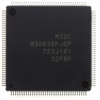
M30835FJGP#U3 Renesas Electronics America, M30835FJGP#U3 Datasheet - Page 253

M30835FJGP#U3
Manufacturer Part Number
M30835FJGP#U3
Description
IC M32C/83 MCU FLASH 144LQFP
Manufacturer
Renesas Electronics America
Series
M16C™ M32C/80r
Datasheets
1.M3087BFLGPU3.pdf
(364 pages)
2.M30833FJGPU3.pdf
(96 pages)
3.M30833FJGPU3.pdf
(529 pages)
Specifications of M30835FJGP#U3
Core Processor
M32C/80
Core Size
16/32-Bit
Speed
32MHz
Connectivity
CAN, I²C, IEBus, SIO, UART/USART
Peripherals
DMA, WDT
Number Of I /o
121
Program Memory Size
512KB (512K x 8)
Program Memory Type
FLASH
Ram Size
31K x 8
Voltage - Supply (vcc/vdd)
3 V ~ 5.5 V
Data Converters
A/D 34x10b, D/A 2x8b
Oscillator Type
Internal
Operating Temperature
-40°C ~ 85°C
Package / Case
144-LQFP
For Use With
R0K330879S001BE - KIT DEV RSK M32C/87R0K330879S000BE - KIT DEV RSK M32C/87
Lead Free Status / RoHS Status
Lead free / RoHS Compliant
Eeprom Size
-
Available stocks
Company
Part Number
Manufacturer
Quantity
Price
- Current page: 253 of 529
- Download datasheet (5Mb)
R
R
M
e
E
. v
3
J
Figure 17.2 AD0CON0 Register
0
2
1
9
C
3 .
B
8 /
0
1
0
3
3
J
G
4
a
0 -
n
o r
A/D0 Control Register 0
b7
3 .
1
u
NOTES:
, 1
3
p
b6
1
4. Set the PSC_7 bit in the PSC register to "1" (AN
6.
1. When the AD0CON0 register is rewritten during the A/D conversion, the conversion result is
2. Analog input pins must be set again after changing A/D operation mode.
3. This bit is disabled in single sweep mode, repeat sweep mode 0 and repeat sweep mode 1.
5. To set the TRG bit to "1", select the cause of trigger by setting the TRG1 and TRG0 bits in the
2
(
0
M
Combination of the CKS0 and CKS1 bits selects
b5
indeterminate.
AD0CON2 register. Then set the ADST bit to "1" after the TRG bit is set to "1".
0
3
CKS0
6
AD
AD
2
b4
0
0
1
1
C
frequency must be under 16 MHz when V
frequency must be under 10 MHz when V
Page 228
8 /
b3
, 3
b2
CKS1
M
0
1
0
1
b1
3
2
b0
C
f o
8 /
f
f
f
4
AD
AD
AD
8
3
Symbol
ADST
CKS0
MD0
MD1
TRG
8
) T
CH0
CH1
CH2
divided by 4
divided by 3
divided by 2
Bit
Symbol
AD0CON0
f
AD
AD
(1)
Analog Input Pin
Select Bit
A/D Operation
Mode Select Bit 0
Trigger Select Bit
A/D Conversion
Start Flag
Frequency Select
Bit
(6)
Bit Name
(2, 3, 4)
Address
0396
CC
CC
4
16
to AN
=5V.
=3.3V.
(2)
AD
.
b2
b4
0 0 0 : AN
0 0 1 : AN
0 1 0 : AN
0 1 1 : AN
1 0 0 : AN
1 0 1 : AN
1 1 0 : AN
1 1 1 : AN
0 0 : One-shot mode
0 1 : Repeat mode
1 0 : Single sweep mode
1 1 : Repeat sweep mode 0 or 1
0 : Software trigger
1 : External trigger, hardware trigger
0 : A/D conversion stops
1 : A/D conversion starts
0 : Select from f
1 : Select from f
7
) to use the P10 pin as a analog input pin.
b1 b0
b3
0
1
2
3
4
5
6
7
AD
AD
After Reset
00
/3 or f
/1 or f
16
Function
AD
AD
(5)
/4
/2
(5)
17. A/D Converter
RW
RW
RW
RW
RW
RW
RW
RW
RW
Related parts for M30835FJGP#U3
Image
Part Number
Description
Manufacturer
Datasheet
Request
R

Part Number:
Description:
KIT STARTER FOR M16C/29
Manufacturer:
Renesas Electronics America
Datasheet:

Part Number:
Description:
KIT STARTER FOR R8C/2D
Manufacturer:
Renesas Electronics America
Datasheet:

Part Number:
Description:
R0K33062P STARTER KIT
Manufacturer:
Renesas Electronics America
Datasheet:

Part Number:
Description:
KIT STARTER FOR R8C/23 E8A
Manufacturer:
Renesas Electronics America
Datasheet:

Part Number:
Description:
KIT STARTER FOR R8C/25
Manufacturer:
Renesas Electronics America
Datasheet:

Part Number:
Description:
KIT STARTER H8S2456 SHARPE DSPLY
Manufacturer:
Renesas Electronics America
Datasheet:

Part Number:
Description:
KIT STARTER FOR R8C38C
Manufacturer:
Renesas Electronics America
Datasheet:

Part Number:
Description:
KIT STARTER FOR R8C35C
Manufacturer:
Renesas Electronics America
Datasheet:

Part Number:
Description:
KIT STARTER FOR R8CL3AC+LCD APPS
Manufacturer:
Renesas Electronics America
Datasheet:

Part Number:
Description:
KIT STARTER FOR RX610
Manufacturer:
Renesas Electronics America
Datasheet:

Part Number:
Description:
KIT STARTER FOR R32C/118
Manufacturer:
Renesas Electronics America
Datasheet:

Part Number:
Description:
KIT DEV RSK-R8C/26-29
Manufacturer:
Renesas Electronics America
Datasheet:

Part Number:
Description:
KIT STARTER FOR SH7124
Manufacturer:
Renesas Electronics America
Datasheet:

Part Number:
Description:
KIT STARTER FOR H8SX/1622
Manufacturer:
Renesas Electronics America
Datasheet:

Part Number:
Description:
KIT DEV FOR SH7203
Manufacturer:
Renesas Electronics America
Datasheet:


