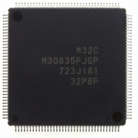
M30835FJGP#U3 Renesas Electronics America, M30835FJGP#U3 Datasheet - Page 431

M30835FJGP#U3
Manufacturer Part Number
M30835FJGP#U3
Description
IC M32C/83 MCU FLASH 144LQFP
Manufacturer
Renesas Electronics America
Series
M16C™ M32C/80r
Datasheets
1.M3087BFLGPU3.pdf
(364 pages)
2.M30833FJGPU3.pdf
(96 pages)
3.M30833FJGPU3.pdf
(529 pages)
Specifications of M30835FJGP#U3
Core Processor
M32C/80
Core Size
16/32-Bit
Speed
32MHz
Connectivity
CAN, I²C, IEBus, SIO, UART/USART
Peripherals
DMA, WDT
Number Of I /o
121
Program Memory Size
512KB (512K x 8)
Program Memory Type
FLASH
Ram Size
31K x 8
Voltage - Supply (vcc/vdd)
3 V ~ 5.5 V
Data Converters
A/D 34x10b, D/A 2x8b
Oscillator Type
Internal
Operating Temperature
-40°C ~ 85°C
Package / Case
144-LQFP
For Use With
R0K330879S001BE - KIT DEV RSK M32C/87R0K330879S000BE - KIT DEV RSK M32C/87
Lead Free Status / RoHS Status
Lead free / RoHS Compliant
Eeprom Size
-
Available stocks
Company
Part Number
Manufacturer
Quantity
Price
- Current page: 431 of 529
- Download datasheet (5Mb)
R
R
M
e
E
3
. v
J
Table 25.5 Errors and Status Register State
NOTES:
2
0
25.3.6 Full Status Check
SR5 SR4 SR3
1
9
C
1
1
0
0
3 .
B
If an error occurs when a program or erase operation is completed, the SR3 to SR5 bits in the status
register are set to "1", indicating a specific error. Therefore, execution results can be confirmed by verify-
ing these bits (full status check).
Table 25.5 lists errors and status register state. Figure 25.12 shows a flow chart of the full status check
and handling procedure for each error.
1. The flash memory enters read array mode when command code "xxFF
2. If the FMR02 bit is set to "1" (lock bit disabled), no error occurs even under the conditions listed above.
8 /
Status Register
0
1
3
0
cycle of these commands. The command code written in the first bus cycle becomes invalid.
3
J
G
4
a
0
1
0
0 -
n
o r
1
3 .
1
u
, 1
3
p
1
2
(
M
0
0
0
0
1
0
3
6
2
C
Command sequence
error
Erase error
Program error
Excessive write error
8 /
Page 406
, 3
M
3
2
Error
C
f o
8 /
4
3
8
) T
8
• The page program command is executed on a locked
• The page program command is executed in an unlocked
• The lock bit program command is executed but the pro-
Excessive write occurs after the page program command
is executed
• An incorrect command is written
• A value other than "xxD0
• The block erase command is executed on a locked block
• The block erase or erase all unlocked block command is
block
block but the program operation is not completed as ex-
pected
gram operation is not completed as expected
ond bus cycle of the lock bit program, block erase or erase
all unlocked block command
executed on an unlock block but the erase operation is not
completed as expected
(2)
Error Occurrence Conditions
16
" or "xxFF
(1)
16
" is written in the second bus
16
25. Flash Memory Version
" is written in the sec-
2
Related parts for M30835FJGP#U3
Image
Part Number
Description
Manufacturer
Datasheet
Request
R

Part Number:
Description:
KIT STARTER FOR M16C/29
Manufacturer:
Renesas Electronics America
Datasheet:

Part Number:
Description:
KIT STARTER FOR R8C/2D
Manufacturer:
Renesas Electronics America
Datasheet:

Part Number:
Description:
R0K33062P STARTER KIT
Manufacturer:
Renesas Electronics America
Datasheet:

Part Number:
Description:
KIT STARTER FOR R8C/23 E8A
Manufacturer:
Renesas Electronics America
Datasheet:

Part Number:
Description:
KIT STARTER FOR R8C/25
Manufacturer:
Renesas Electronics America
Datasheet:

Part Number:
Description:
KIT STARTER H8S2456 SHARPE DSPLY
Manufacturer:
Renesas Electronics America
Datasheet:

Part Number:
Description:
KIT STARTER FOR R8C38C
Manufacturer:
Renesas Electronics America
Datasheet:

Part Number:
Description:
KIT STARTER FOR R8C35C
Manufacturer:
Renesas Electronics America
Datasheet:

Part Number:
Description:
KIT STARTER FOR R8CL3AC+LCD APPS
Manufacturer:
Renesas Electronics America
Datasheet:

Part Number:
Description:
KIT STARTER FOR RX610
Manufacturer:
Renesas Electronics America
Datasheet:

Part Number:
Description:
KIT STARTER FOR R32C/118
Manufacturer:
Renesas Electronics America
Datasheet:

Part Number:
Description:
KIT DEV RSK-R8C/26-29
Manufacturer:
Renesas Electronics America
Datasheet:

Part Number:
Description:
KIT STARTER FOR SH7124
Manufacturer:
Renesas Electronics America
Datasheet:

Part Number:
Description:
KIT STARTER FOR H8SX/1622
Manufacturer:
Renesas Electronics America
Datasheet:

Part Number:
Description:
KIT DEV FOR SH7203
Manufacturer:
Renesas Electronics America
Datasheet:


