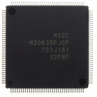
M30835FJGP#U3 Renesas Electronics America, M30835FJGP#U3 Datasheet - Page 384

M30835FJGP#U3
Manufacturer Part Number
M30835FJGP#U3
Description
IC M32C/83 MCU FLASH 144LQFP
Manufacturer
Renesas Electronics America
Series
M16C™ M32C/80r
Datasheets
1.M3087BFLGPU3.pdf
(364 pages)
2.M30833FJGPU3.pdf
(96 pages)
3.M30833FJGPU3.pdf
(529 pages)
Specifications of M30835FJGP#U3
Core Processor
M32C/80
Core Size
16/32-Bit
Speed
32MHz
Connectivity
CAN, I²C, IEBus, SIO, UART/USART
Peripherals
DMA, WDT
Number Of I /o
121
Program Memory Size
512KB (512K x 8)
Program Memory Type
FLASH
Ram Size
31K x 8
Voltage - Supply (vcc/vdd)
3 V ~ 5.5 V
Data Converters
A/D 34x10b, D/A 2x8b
Oscillator Type
Internal
Operating Temperature
-40°C ~ 85°C
Package / Case
144-LQFP
For Use With
R0K330879S001BE - KIT DEV RSK M32C/87R0K330879S000BE - KIT DEV RSK M32C/87
Lead Free Status / RoHS Status
Lead free / RoHS Compliant
Eeprom Size
-
Available stocks
Company
Part Number
Manufacturer
Quantity
Price
- Current page: 384 of 529
- Download datasheet (5Mb)
R
R
M
23. DRAMC
e
E
3
. v
J
NOTES:
Table 23.1 DRAMC Specifications
Table 23.2 DRAMC-associated Pins
2
0
The DRAM controller (DRAMC) controls the DRAM area, which ranges from 512 Kbytes to 8 Mbytes. Table
23.1 lists specifications of the DRAMC.
DRAM Area
Bus Control
Refresh
Supported Function Mode EDO, fast page mode
Wait State Insertion
Table 23.2 shows pins associated with DRAMC. Signals listed in Table 23.2 are output by setting the AR2
to AR0 bits in the DRAMCONT register for the DRAM area and accessing DRAM. See Table 7.9 for RAS,
CASL, CASH and DW signal operations. Figure 23.1 shows the DRAMCONT register and REFCNT regis-
ter.
1
C
9
________
P0
P1
P3
P4
P5
P5
P5
P5
3 .
B
8 /
1. This is an example of the separate bus and 16-bit data bus.
2. This bus is available when the DS2 bit in the DS register is set to "1" (16-bit data bus) and the PM02 bit
0
1
3
0
0
0
1
2
6
in the PM0 register is set to "1" (RD/WRL/WRH in R/W mode).
3
J
Port
to P4
G
4
a
0 -
n
o r
________
3 .
1
u
, 1
3
Item
p
4
1
2
(
M
0
0
3
6
2
C
_____
Page 359
8 /
D
D
A
A
WRL / WR
WRH / BHE
RD
ALE
________
_______
____
, 3
8
16
0
8
Bus for Device Access except DRAM
to D
to D
to D
M
to A
3
2
15
_____
7
15
_______
________
20
512 KB, 1 MB, 2 MB, 4 MB, 8 MB
2CAS/1W
CAS-before-RAS refresh, Self refresh
1-wait state, 2-wait state
C
f o
8 /
4
3
8
) T
8
____
________
_______
_______
Specification
(1)
D
D
MA
MA
CASL
CASH
DW
RAS
_________
_______
_________
_____
0
8
to D
to D
0
8
to MA
to MA
Bus for DRAM Access
7
15 (2)
7
12
23. DRAMC
______
Related parts for M30835FJGP#U3
Image
Part Number
Description
Manufacturer
Datasheet
Request
R

Part Number:
Description:
KIT STARTER FOR M16C/29
Manufacturer:
Renesas Electronics America
Datasheet:

Part Number:
Description:
KIT STARTER FOR R8C/2D
Manufacturer:
Renesas Electronics America
Datasheet:

Part Number:
Description:
R0K33062P STARTER KIT
Manufacturer:
Renesas Electronics America
Datasheet:

Part Number:
Description:
KIT STARTER FOR R8C/23 E8A
Manufacturer:
Renesas Electronics America
Datasheet:

Part Number:
Description:
KIT STARTER FOR R8C/25
Manufacturer:
Renesas Electronics America
Datasheet:

Part Number:
Description:
KIT STARTER H8S2456 SHARPE DSPLY
Manufacturer:
Renesas Electronics America
Datasheet:

Part Number:
Description:
KIT STARTER FOR R8C38C
Manufacturer:
Renesas Electronics America
Datasheet:

Part Number:
Description:
KIT STARTER FOR R8C35C
Manufacturer:
Renesas Electronics America
Datasheet:

Part Number:
Description:
KIT STARTER FOR R8CL3AC+LCD APPS
Manufacturer:
Renesas Electronics America
Datasheet:

Part Number:
Description:
KIT STARTER FOR RX610
Manufacturer:
Renesas Electronics America
Datasheet:

Part Number:
Description:
KIT STARTER FOR R32C/118
Manufacturer:
Renesas Electronics America
Datasheet:

Part Number:
Description:
KIT DEV RSK-R8C/26-29
Manufacturer:
Renesas Electronics America
Datasheet:

Part Number:
Description:
KIT STARTER FOR SH7124
Manufacturer:
Renesas Electronics America
Datasheet:

Part Number:
Description:
KIT STARTER FOR H8SX/1622
Manufacturer:
Renesas Electronics America
Datasheet:

Part Number:
Description:
KIT DEV FOR SH7203
Manufacturer:
Renesas Electronics America
Datasheet:


