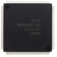
M30835FJGP#U3 Renesas Electronics America, M30835FJGP#U3 Datasheet - Page 490

M30835FJGP#U3
Manufacturer Part Number
M30835FJGP#U3
Description
IC M32C/83 MCU FLASH 144LQFP
Manufacturer
Renesas Electronics America
Series
M16C™ M32C/80r
Datasheets
1.M3087BFLGPU3.pdf
(364 pages)
2.M30833FJGPU3.pdf
(96 pages)
3.M30833FJGPU3.pdf
(529 pages)
Specifications of M30835FJGP#U3
Core Processor
M32C/80
Core Size
16/32-Bit
Speed
32MHz
Connectivity
CAN, I²C, IEBus, SIO, UART/USART
Peripherals
DMA, WDT
Number Of I /o
121
Program Memory Size
512KB (512K x 8)
Program Memory Type
FLASH
Ram Size
31K x 8
Voltage - Supply (vcc/vdd)
3 V ~ 5.5 V
Data Converters
A/D 34x10b, D/A 2x8b
Oscillator Type
Internal
Operating Temperature
-40°C ~ 85°C
Package / Case
144-LQFP
For Use With
R0K330879S001BE - KIT DEV RSK M32C/87R0K330879S000BE - KIT DEV RSK M32C/87
Lead Free Status / RoHS Status
Lead free / RoHS Compliant
Eeprom Size
-
Available stocks
Company
Part Number
Manufacturer
Quantity
Price
- Current page: 490 of 529
- Download datasheet (5Mb)
R
R
M
27.4 Clock Generation Circuit
e
E
3
. v
J
2
0
27.4.1 PLL Frequency Synthesizer
27.4.2 Power Consumption Control
C
1
9
3 .
B
8 /
Stabilize supply voltage when using the PLL frequency synthesizer. The ripple of supply voltage at 5V
must be less than 10kHz in frequency, 0.5V (peak to peak) in voltage fluctuation range, and 1V/ms in
voltage fluctuation rate. The ripple of supply voltage at 3.3V must be less than 100Hz in frequency, 0.2V
(peak to peak) in voltage fluctuation range, and 0.1V/ms in voltage fluctuation rate.
• When resetting the microcomputer to exit stop mode, apply an "L" signal to the RESET pin until the main
• Write at least 4 NOP instructions after the WAIT instruction or instructions to set the CM10 bit in the CM1
• The followings are suggestions for reducing power consumption when programming or designing sys-
0
1
clock oscillation stabilizes.
register to "1" (all clocks stop). When entering wait mode or stop mode, the instruction queue reads
ahead to instructions following the WAIT instruction and instructions to set the CM10 bit to "1", and the
program stops. The next instruction may be executed before entering wait mode or stop mode, depend-
ing on the combination of instructions and their execution timing.
tems:
3
0
Ports: I/O ports maintains the same state despite the microcomputer entering wait mode or stop
mode. Current flows through active output ports. Feedthrough current flows through input ports in a
high-impedance state. Set unused ports as input ports and stablize electrical potential before entering
wait mode or stop mode.
A/D Converter: If the A/D conversion is not performed, set the VCUT bit in the AD0CON1 register to
"0"(no V
starting the A/D conversion.
D/A Converter: Set the DAi bit (i=0 to 1) in the DACON register to "0" (output disabled) and set the
DAi register to "00
Peripheral Function Stop: Set the CM02 bit in the CM0 register while in wait mode to stop unneces-
sary peripheral functions. However, this does not reduce power consumption because the peripheral
function clock (fc32) generating from the sub clock does not stop. When in low-speed mode and low-
power consumption mode, do not enter wait mode when the CM02 bit is set to "1" (peripheral clock
stops in wait mode).
External Clock: When an external clock is selected as the CPU clock, set the CM05 bit in the CM0
register to "1" (main clock stops). This disables the X
using an external clock input, the clock is applied regardless of the CM05 bit setting.)
3
J
G
4
a
o r
0 -
n
3 .
1
u
, 1
3
p
1
(
2
M
REF
0
0
3
6
2
C
connection). Set the VCUT bit to "1" (V
Page 465
8 /
, 3
16
M
" when the D/A conversion is not performed.
3
2
C
f o
8 /
4
3
8
) T
8
OUT
REF
pin and reduces power consumption. (When
connection) and wait at least 1 s before
27. Precautions (Clock Generation Circuit)
____________
Related parts for M30835FJGP#U3
Image
Part Number
Description
Manufacturer
Datasheet
Request
R

Part Number:
Description:
KIT STARTER FOR M16C/29
Manufacturer:
Renesas Electronics America
Datasheet:

Part Number:
Description:
KIT STARTER FOR R8C/2D
Manufacturer:
Renesas Electronics America
Datasheet:

Part Number:
Description:
R0K33062P STARTER KIT
Manufacturer:
Renesas Electronics America
Datasheet:

Part Number:
Description:
KIT STARTER FOR R8C/23 E8A
Manufacturer:
Renesas Electronics America
Datasheet:

Part Number:
Description:
KIT STARTER FOR R8C/25
Manufacturer:
Renesas Electronics America
Datasheet:

Part Number:
Description:
KIT STARTER H8S2456 SHARPE DSPLY
Manufacturer:
Renesas Electronics America
Datasheet:

Part Number:
Description:
KIT STARTER FOR R8C38C
Manufacturer:
Renesas Electronics America
Datasheet:

Part Number:
Description:
KIT STARTER FOR R8C35C
Manufacturer:
Renesas Electronics America
Datasheet:

Part Number:
Description:
KIT STARTER FOR R8CL3AC+LCD APPS
Manufacturer:
Renesas Electronics America
Datasheet:

Part Number:
Description:
KIT STARTER FOR RX610
Manufacturer:
Renesas Electronics America
Datasheet:

Part Number:
Description:
KIT STARTER FOR R32C/118
Manufacturer:
Renesas Electronics America
Datasheet:

Part Number:
Description:
KIT DEV RSK-R8C/26-29
Manufacturer:
Renesas Electronics America
Datasheet:

Part Number:
Description:
KIT STARTER FOR SH7124
Manufacturer:
Renesas Electronics America
Datasheet:

Part Number:
Description:
KIT STARTER FOR H8SX/1622
Manufacturer:
Renesas Electronics America
Datasheet:

Part Number:
Description:
KIT DEV FOR SH7203
Manufacturer:
Renesas Electronics America
Datasheet:


