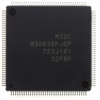
M30835FJGP#U3 Renesas Electronics America, M30835FJGP#U3 Datasheet - Page 523

M30835FJGP#U3
Manufacturer Part Number
M30835FJGP#U3
Description
IC M32C/83 MCU FLASH 144LQFP
Manufacturer
Renesas Electronics America
Series
M16C™ M32C/80r
Datasheets
1.M3087BFLGPU3.pdf
(364 pages)
2.M30833FJGPU3.pdf
(96 pages)
3.M30833FJGPU3.pdf
(529 pages)
Specifications of M30835FJGP#U3
Core Processor
M32C/80
Core Size
16/32-Bit
Speed
32MHz
Connectivity
CAN, I²C, IEBus, SIO, UART/USART
Peripherals
DMA, WDT
Number Of I /o
121
Program Memory Size
512KB (512K x 8)
Program Memory Type
FLASH
Ram Size
31K x 8
Voltage - Supply (vcc/vdd)
3 V ~ 5.5 V
Data Converters
A/D 34x10b, D/A 2x8b
Oscillator Type
Internal
Operating Temperature
-40°C ~ 85°C
Package / Case
144-LQFP
For Use With
R0K330879S001BE - KIT DEV RSK M32C/87R0K330879S000BE - KIT DEV RSK M32C/87
Lead Free Status / RoHS Status
Lead free / RoHS Compliant
Eeprom Size
-
Available stocks
Company
Part Number
Manufacturer
Quantity
Price
- Current page: 523 of 529
- Download datasheet (5Mb)
Rev.
REVISION HISTORY
Date
Page
325
344
345
346
364
365
367
369
371
372
376
377
378
379
383
384
387
389
393
395
397
405
406
412
• 22.1.1.3 BASICCAN Bit revised
• 22.1.16 CANi Message Slotj Control Register (CiMCTLj Register) (i=0, 1;
• Table 22.4 C0MCTLi Register (i=0 to 15) Setting and Transmit/Receive
• 22.1.16.4 REMACTIVE Bit revised
• 22.1.16.5 RSPLOCK Bit revised
Programmable I/O Port
• 24.4 Function Select Register Bk (PSLk Register) (k=0 to 3) revised
• 24.5 Function Select Register C (PSC Register) revised
• 24.7 Port Control Register (PCR Register) revised
• Figure 24.2 Programmable I/O Ports (2) modified
• Figure 24.5 PD0 to PD15 Registers Note 4 added
• Figure 24.7 PS0 Register and PS1 Register PS0 register revised
• Figure 24.8 PS2 Register and PS3 Register PS3 register revised
• Figure 24.12 PSL0 Register and PSL1 Register Note 1 added to PSL1
• Figure 24.13 PSL2 Register and PSL3 Register PSL3 register revised
• Figure 24.14 PSC Register revised
• Figure 24.15 PUR0 Register, PUR1 Register and PUR2 Register Note 1
• Table 24.3 Port P6 Peripheral Function Output Control Bits 3 and 7
• Table 24.4 Port P7 Peripheral Function Output Control Note 1 added to
• Table 24.6 Port P9 Peripheral Function Output Control Bit 2 and 6 modified
Flash Memory Version
• Table 25.1 Flash Memory Version Specifications Supply voltage modified
• 25.2.1 ROM Code Protect Function revised
• 25.2.2 ID Code Check Function revised
• 25.3.1.3 FMR02 Bit revised
• 25.3.3 Data Protect Function revised
• 25.3.5.3 Clear status Register revised
• 25.3.7.8 Rewriting the User ROM Area
• 25.4.2 ID Code Check Function revised
• 25.5.2 ROM Code Protect Function revised
j=0 to 15) Funtion of the INVALDATA/TRMACTIVE bit when set to “1” changed
to “Transmits”; Note 4 in REMACTIVE deleted; RW modified to RO
Mode Hyphens (-) changed to “0”
register
revised
modified
PSC register; Bit 0 modified
M32C/83 GROUP (M32C/83, M32C/83T) Hardware Manual
C-10
Description
Summary
Related parts for M30835FJGP#U3
Image
Part Number
Description
Manufacturer
Datasheet
Request
R

Part Number:
Description:
KIT STARTER FOR M16C/29
Manufacturer:
Renesas Electronics America
Datasheet:

Part Number:
Description:
KIT STARTER FOR R8C/2D
Manufacturer:
Renesas Electronics America
Datasheet:

Part Number:
Description:
R0K33062P STARTER KIT
Manufacturer:
Renesas Electronics America
Datasheet:

Part Number:
Description:
KIT STARTER FOR R8C/23 E8A
Manufacturer:
Renesas Electronics America
Datasheet:

Part Number:
Description:
KIT STARTER FOR R8C/25
Manufacturer:
Renesas Electronics America
Datasheet:

Part Number:
Description:
KIT STARTER H8S2456 SHARPE DSPLY
Manufacturer:
Renesas Electronics America
Datasheet:

Part Number:
Description:
KIT STARTER FOR R8C38C
Manufacturer:
Renesas Electronics America
Datasheet:

Part Number:
Description:
KIT STARTER FOR R8C35C
Manufacturer:
Renesas Electronics America
Datasheet:

Part Number:
Description:
KIT STARTER FOR R8CL3AC+LCD APPS
Manufacturer:
Renesas Electronics America
Datasheet:

Part Number:
Description:
KIT STARTER FOR RX610
Manufacturer:
Renesas Electronics America
Datasheet:

Part Number:
Description:
KIT STARTER FOR R32C/118
Manufacturer:
Renesas Electronics America
Datasheet:

Part Number:
Description:
KIT DEV RSK-R8C/26-29
Manufacturer:
Renesas Electronics America
Datasheet:

Part Number:
Description:
KIT STARTER FOR SH7124
Manufacturer:
Renesas Electronics America
Datasheet:

Part Number:
Description:
KIT STARTER FOR H8SX/1622
Manufacturer:
Renesas Electronics America
Datasheet:

Part Number:
Description:
KIT DEV FOR SH7203
Manufacturer:
Renesas Electronics America
Datasheet:


