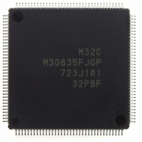
M30835FJGP#U3 Renesas Electronics America, M30835FJGP#U3 Datasheet - Page 516

M30835FJGP#U3
Manufacturer Part Number
M30835FJGP#U3
Description
IC M32C/83 MCU FLASH 144LQFP
Manufacturer
Renesas Electronics America
Series
M16C™ M32C/80r
Datasheets
1.M3087BFLGPU3.pdf
(364 pages)
2.M30833FJGPU3.pdf
(96 pages)
3.M30833FJGPU3.pdf
(529 pages)
Specifications of M30835FJGP#U3
Core Processor
M32C/80
Core Size
16/32-Bit
Speed
32MHz
Connectivity
CAN, I²C, IEBus, SIO, UART/USART
Peripherals
DMA, WDT
Number Of I /o
121
Program Memory Size
512KB (512K x 8)
Program Memory Type
FLASH
Ram Size
31K x 8
Voltage - Supply (vcc/vdd)
3 V ~ 5.5 V
Data Converters
A/D 34x10b, D/A 2x8b
Oscillator Type
Internal
Operating Temperature
-40°C ~ 85°C
Package / Case
144-LQFP
For Use With
R0K330879S001BE - KIT DEV RSK M32C/87R0K330879S000BE - KIT DEV RSK M32C/87
Lead Free Status / RoHS Status
Lead free / RoHS Compliant
Eeprom Size
-
Available stocks
Company
Part Number
Manufacturer
Quantity
Price
- Current page: 516 of 529
- Download datasheet (5Mb)
Rev.
REVISION HISTORY
Date
Page
207
216
226
296
304
315
317
320
324
334
364
385
388
390
391
393
394
398
400
429
• Modify PD7_2=0 to PD7_0=0 on ‘PD7 register’ column and ‘SRxD2 input’ row in
• Modify PD7_0=0 to PD7_2=0 on ‘PD7 register’ column and ‘CLK2 input’ row in
• Modify PS3_4=0 to PS3_5=0 on ‘PS3 register’ column and ‘CLK4 input’ row in
CAN Module
• Modify PSL2_2=0 to PSL2_1=0 on ‘PSL1 and PSL2 registers’ column and ‘P8
Intelligent I/O
• Modify Setting value of the GiPO0 register to Setting value of the GiPOk register
• Modify RxD to ISRxD on ‘IPOL’ row and TxD to ISTxD on ‘OPOL’ row in Figure
• Modify IPS=1 to IPS1=1 on IPS registers column and ‘P11
• Modify TCRCRC to TCRCE on ‘CRC’ row in Table 1.22.28.
• Delete SIOiTR and SIOiRR and add SRTiR in note 3 in Table 1.22.28.
• Modify IER to OER in note 1 in the second figure of Figure 1.22.42.
• Modify SIOiTR to SIO2TR and SIO5RR to SIO2RR in Table 1.22.30 and 1.22.36.
• Modify GiCR to G3CR in Table 1.22.41.
DRAMC
• Modify SRDF to SREF in note 3 in Figure 1.27.1.
• Modify IOUTC1
• Modify P0 to P5 to P1 in note 1 in Table 1.28.17.
Programable I/O Port
• Modify INPC
• Modify INPC
• Modify ISCLK input to ISCLK0 input on ‘Bit 1’ row in table 1.28.12.
Usage Precaution
• Modify PM0 to PM00 in “HOLD Signal”
• Modify all SP to ISP in (1) SP Setting of “Interrupts”.
• Modify all TAi to TBi in 1. Timer Mode and Event Counter Mode of “Timer B”.
• Modify the CAN module to the microcomputer in “Resetting CNVSS Pin with H”.
• Delete a discription of ‘Difference between Flash Memory version and Masked
Electric Charactistics
• Modify IOH=5mA to IOL=5mA on ‘VOL’ row and ‘Mesurement Condition’ column
Table 1.20.11.
Table 1.20.11.
Table 1.20.23.
row in Table 1.21.2.
as n and m on the second figure in Figure 1.22.26.
1.22.33.
1.22.26.
ROM’
in Table 1.31.3.
M32C/83 GROUP (M32C/83, M32C/83T) Hardware Manual
1
0
to INPC1
to INPC0
0
to OUTC1
C-3
1
2
on ‘PS1 register’ column and ‘Bit 4’ row in Table 1.28.4.
on ‘PS2 register’ column and ‘Bit 0’ row in table 1.28.5.
_________
0
Description
on ‘PSC_3’ row in Figure 1.28.14.
Summary
2
’ row in Table
2
’
Related parts for M30835FJGP#U3
Image
Part Number
Description
Manufacturer
Datasheet
Request
R

Part Number:
Description:
KIT STARTER FOR M16C/29
Manufacturer:
Renesas Electronics America
Datasheet:

Part Number:
Description:
KIT STARTER FOR R8C/2D
Manufacturer:
Renesas Electronics America
Datasheet:

Part Number:
Description:
R0K33062P STARTER KIT
Manufacturer:
Renesas Electronics America
Datasheet:

Part Number:
Description:
KIT STARTER FOR R8C/23 E8A
Manufacturer:
Renesas Electronics America
Datasheet:

Part Number:
Description:
KIT STARTER FOR R8C/25
Manufacturer:
Renesas Electronics America
Datasheet:

Part Number:
Description:
KIT STARTER H8S2456 SHARPE DSPLY
Manufacturer:
Renesas Electronics America
Datasheet:

Part Number:
Description:
KIT STARTER FOR R8C38C
Manufacturer:
Renesas Electronics America
Datasheet:

Part Number:
Description:
KIT STARTER FOR R8C35C
Manufacturer:
Renesas Electronics America
Datasheet:

Part Number:
Description:
KIT STARTER FOR R8CL3AC+LCD APPS
Manufacturer:
Renesas Electronics America
Datasheet:

Part Number:
Description:
KIT STARTER FOR RX610
Manufacturer:
Renesas Electronics America
Datasheet:

Part Number:
Description:
KIT STARTER FOR R32C/118
Manufacturer:
Renesas Electronics America
Datasheet:

Part Number:
Description:
KIT DEV RSK-R8C/26-29
Manufacturer:
Renesas Electronics America
Datasheet:

Part Number:
Description:
KIT STARTER FOR SH7124
Manufacturer:
Renesas Electronics America
Datasheet:

Part Number:
Description:
KIT STARTER FOR H8SX/1622
Manufacturer:
Renesas Electronics America
Datasheet:

Part Number:
Description:
KIT DEV FOR SH7203
Manufacturer:
Renesas Electronics America
Datasheet:


