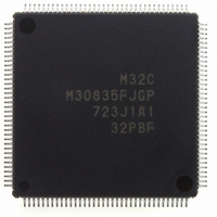
M30835FJGP#U3 Renesas Electronics America, M30835FJGP#U3 Datasheet - Page 335

M30835FJGP#U3
Manufacturer Part Number
M30835FJGP#U3
Description
IC M32C/83 MCU FLASH 144LQFP
Manufacturer
Renesas Electronics America
Series
M16C™ M32C/80r
Datasheets
1.M3087BFLGPU3.pdf
(364 pages)
2.M30833FJGPU3.pdf
(96 pages)
3.M30833FJGPU3.pdf
(529 pages)
Specifications of M30835FJGP#U3
Core Processor
M32C/80
Core Size
16/32-Bit
Speed
32MHz
Connectivity
CAN, I²C, IEBus, SIO, UART/USART
Peripherals
DMA, WDT
Number Of I /o
121
Program Memory Size
512KB (512K x 8)
Program Memory Type
FLASH
Ram Size
31K x 8
Voltage - Supply (vcc/vdd)
3 V ~ 5.5 V
Data Converters
A/D 34x10b, D/A 2x8b
Oscillator Type
Internal
Operating Temperature
-40°C ~ 85°C
Package / Case
144-LQFP
For Use With
R0K330879S001BE - KIT DEV RSK M32C/87R0K330879S000BE - KIT DEV RSK M32C/87
Lead Free Status / RoHS Status
Lead free / RoHS Compliant
Eeprom Size
-
Available stocks
Company
Part Number
Manufacturer
Quantity
Price
- Current page: 335 of 529
- Download datasheet (5Mb)
M
R
R
e
E
3
. v
J
2
NOTES:
Table 21.30 Variable Clock Synchronous Serial I/O Mode Specifications (Group 2)
9 0
C
Transfer Clock
Transmit Start Condition
Receive Start Condition
Interrupt Request
Error Detection
Selectable Function
21.5.1 Variable Clock Synchronous Serial I/O Mode (Group 2)
Transfer Data Format
. 1
1. The transfer clock must be f
2. Transfer clocks must be f
3. When an overrun error occurs, the G2RB register is indeterminate.
8 /
B
In variable clock synchronous serial I/O mode, data is transmitted and received using the transfer clock.
The length of data transferred is selected from 1 to 8 bits. Table 21.30 lists specifications of the group 2
variable clock synchronous serial I/O mode. Table 21.31 lists registers to be used and their settings.
Tables 21.32 to 21.35 lists pin settings. Figure 21.46 shows an example of a transmit and receive
operation.
1 3
0
3
transmitted. Under conditions other than this, the transfer clock must be f
3 0
G
J
- 4
n a
o r
1 0
3 .
u
p
, 1
1 3
Item
(
0 2
M
(1)
3
6 0
2
C
8 /
Page 310
, 3
M
3
2
• Transfer data length : 1 to 8 bits
• When the CKDIR bit in the G2MR register is set to "0" (internal clock) :
• When the CKDIR bit is set to "1" (external clock) : input from the ISCLK2 pin
• To start transmitting, the following conditions are required :
• To start receiving, the following conditions are required :
• While transmitting, one of the following conditions can be selected to set the
• While receiving, the following condition can be selected to set the SIO2RR bit in the
Overrun error
This error occurs when receiving the j bit (j=1 to 8) of the next data (transfer data
length: j bits) before reading the G2RB register
• LSB first/MSB first
• ISTxD2 and ISRxD2 I/O polarity inverse
• Data transfer bit length
C
- Set the TE bit in the G2CR register to "1" (transmit enable)
- Write data to the G2TB register
- Set the RE bit in the G2CR register to "1" (receive enable)
- Set the TE bit in the G2CR register to "1" (transmit enable)
- Write data to the G2TB register
- The IRS bit in the G2MR register is set to "0" (no data in the G2TB register):
- The IRS bit is set to "1" (reception completed):
when data is transferred from the receive register to the G2RB register (data recep-
The G2PO0 register determines bit rate and the transfer clock is generated in
SIO2TR bit in the IIO6IR register to "1" (see Figure 10.14):
IIO5IR register to "1" (interrupt request) (see Figure 10.14):
tion is completed)
f o
ISTxD2 pin output level and ISRxD2 pin input level are inversed
phase-delayed waveform output mode of the channel 2 waveform generation func-
tion.
n : setting value of the G2PO0 register 0000
Select from 1 to 8 bits
8 /
BT2
when data transfer from the transmit register is completed
Select either bit 0 or bit 7 to transmit/receive data
when data is transferred from the G2TB register to the transmit register.
4
3
BT2
8 8
) T
divided by 20 or more.
divided by six or more when both transfer clock and transfer data are
(3)
21. Intelligent I/O (Group 2 Communication Function)
Specification
16
to FFFF
BT2
16
divided by 20 or more.
2(n+2)
f
BT2
(2)
Related parts for M30835FJGP#U3
Image
Part Number
Description
Manufacturer
Datasheet
Request
R

Part Number:
Description:
KIT STARTER FOR M16C/29
Manufacturer:
Renesas Electronics America
Datasheet:

Part Number:
Description:
KIT STARTER FOR R8C/2D
Manufacturer:
Renesas Electronics America
Datasheet:

Part Number:
Description:
R0K33062P STARTER KIT
Manufacturer:
Renesas Electronics America
Datasheet:

Part Number:
Description:
KIT STARTER FOR R8C/23 E8A
Manufacturer:
Renesas Electronics America
Datasheet:

Part Number:
Description:
KIT STARTER FOR R8C/25
Manufacturer:
Renesas Electronics America
Datasheet:

Part Number:
Description:
KIT STARTER H8S2456 SHARPE DSPLY
Manufacturer:
Renesas Electronics America
Datasheet:

Part Number:
Description:
KIT STARTER FOR R8C38C
Manufacturer:
Renesas Electronics America
Datasheet:

Part Number:
Description:
KIT STARTER FOR R8C35C
Manufacturer:
Renesas Electronics America
Datasheet:

Part Number:
Description:
KIT STARTER FOR R8CL3AC+LCD APPS
Manufacturer:
Renesas Electronics America
Datasheet:

Part Number:
Description:
KIT STARTER FOR RX610
Manufacturer:
Renesas Electronics America
Datasheet:

Part Number:
Description:
KIT STARTER FOR R32C/118
Manufacturer:
Renesas Electronics America
Datasheet:

Part Number:
Description:
KIT DEV RSK-R8C/26-29
Manufacturer:
Renesas Electronics America
Datasheet:

Part Number:
Description:
KIT STARTER FOR SH7124
Manufacturer:
Renesas Electronics America
Datasheet:

Part Number:
Description:
KIT STARTER FOR H8SX/1622
Manufacturer:
Renesas Electronics America
Datasheet:

Part Number:
Description:
KIT DEV FOR SH7203
Manufacturer:
Renesas Electronics America
Datasheet:


