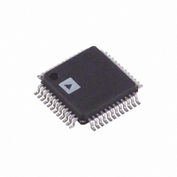
ADUC7032BSTZ-8V-RL Analog Devices Inc, ADUC7032BSTZ-8V-RL Datasheet - Page 14

ADUC7032BSTZ-8V-RL
Manufacturer Part Number
ADUC7032BSTZ-8V-RL
Description
IC BATTERY SENSOR PREC 48-LQFP
Manufacturer
Analog Devices Inc
Series
MicroConverter® ADuC7xxxr
Datasheet
1.ADUC7032BSTZ-8V-RL.pdf
(128 pages)
Specifications of ADUC7032BSTZ-8V-RL
Core Processor
ARM7
Core Size
16/32-Bit
Speed
20.48MHz
Connectivity
LIN, SPI, UART/USART
Peripherals
POR, PSM, Temp Sensor, WDT
Number Of I /o
9
Program Memory Size
96KB (96K x 8)
Program Memory Type
FLASH
Ram Size
6K x 8
Voltage - Supply (vcc/vdd)
3.5 V ~ 18 V
Data Converters
A/D 2x16b
Oscillator Type
Internal
Operating Temperature
-40°C ~ 105°C
Package / Case
48-LQFP
Lead Free Status / RoHS Status
Lead free / RoHS Compliant
Eeprom Size
-
Other names
ADUC7032BSTZ-8V-RLCT
Available stocks
Company
Part Number
Manufacturer
Quantity
Price
Company:
Part Number:
ADUC7032BSTZ-8V-RL
Manufacturer:
Analog Devices Inc
Quantity:
10 000
Parameter
Preliminary Technical Data
1
2
3
4
5
6
7
8
9
10
11
12
13
14
15
16
17
18
19
20
21
22
23
24
25
26
27
28
29
30
31
32
33
34
35
36
These numbers are not production tested but are guaranteed by design and/or characterization data at production release
Valid for Current ADC Gain setting of PGA=4 to 64
Tested at Gain Range=4, Self-Offset Calibration will remove this error.
Measured with an internal short after an initial offset calibration.
Measured with an internal short
These numbers include internal reference temperature drift.
Factory Calibrated at Gain = 1.
System calibration at specific gain range will remove the error at this gain range
input referred noise figures
can also be used to reduce the ADC Input Range (LSB Size).
These numbers include temperature drift
When used in conjunction with ADCREF, the Low Power Mode Reference error MMR.
Using ADC Normal Mode Voltage Reference
Typical Noise in Low Power modes is measured with Chop enabled.
Voltage Channel Specifications include resistive attenuator input stage
System Calibration will remove this error
rms noise is referred to Voltage attenuator input, for example at F
ADC Self Offset calibration will remove this error.
Valid after an initial Self Calibration
Factory calibrated for the internal temperature sensor during final production test.
System Calibration will remove this error
In ADC Low Power Mode the input range is fixed at ±9.375mV. In ADC Low Power Plus Mode the input range is fixed at ±2.34375mV.
It is possible to extend the ADC input range by up to 10% by modifying the factory set value of the Gain Calibration register or using system calibration. This approach
Limited by minimum absolute input voltage range.
Valid for a differential input less than 10mV
Measured using Box Method
The long-term stability specification is non cumulative. The drift in subsequent 1,000 hour periods is significantly lower than in the first 1,000 hour period.
References of up to REG_AVDD can be accommodated by enabling an internal Divide-by-2
Die Temperature.
Endurance is qualified to 10,000 cycles as per JEDEC Std. 22 method A117 and measured at -40°C, +25°C and +125°C. Typical endurance at 25°C is 170,000 cycles.
Retention lifetime equivalent at junction temperature (Tj) = 85°C as per JEDEC Std. 22 method A117. Retention lifetime will de-rate with junction temperature.
Low Power oscillator can be calibrated against either the precision oscillator or the external 32.768kHz crystal in user code
These numbers are not production tested, but are supported by LIN Compliance testing.
Specified after Rlimit of 39Ohms
The MCU core is not shutdown but an interrupt is generated, if enabled.
Thermal Impedance can be used to calculate the thermal gradient from ambient to die temperature.
Typical, additional supply current consumed during Flash memory program and erase cycles is 7mA and 5mA respectively.
Internal Regulated Supply available at REG_DVDD (I
I
I
I
I
I
I
DD
DD
DD
DD
DD
DD
– MCU Powered Down
– MCU Powered Down
– MCU Powered Down
– Current ADC
– Voltage/Temperature ADC
– Precision Oscillator
1
1
Test Conditions/Comments
ADC Low Power-Plus Mode, measured over an
ambient temperature range of -10°C to +40°C
(Continuous ADC Conversion )
Average Current, Measured with Wake and
Watchdog Timer clocked from Low Power
Oscillator
Average Current, Measured with Wake and
Watchdog Timer clocked from Low Power
Oscillator over an ambient temperature range of
-10°C to +40°C
Per ADC
SOURCE
=5mA), and REG_AVDD (I
ADC
=1KHz, typical rms noise at the ADC input is 7.5uV, scaled by the attenuator (24) yields these
Rev. PrD | Page 14 of 128
SOURCE
=1mA)
Min
Typ
520
120
120
1.7
0.5
400
Max
700
300
175
ADuC7032
Unit
µA
µA
µA
mA
mA
µA


