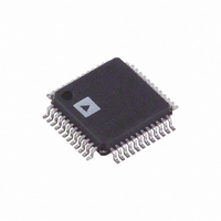
ADUC7032BSTZ-8V-RL Analog Devices Inc, ADUC7032BSTZ-8V-RL Datasheet - Page 69

ADUC7032BSTZ-8V-RL
Manufacturer Part Number
ADUC7032BSTZ-8V-RL
Description
IC BATTERY SENSOR PREC 48-LQFP
Manufacturer
Analog Devices Inc
Series
MicroConverter® ADuC7xxxr
Datasheet
1.ADUC7032BSTZ-8V-RL.pdf
(128 pages)
Specifications of ADUC7032BSTZ-8V-RL
Core Processor
ARM7
Core Size
16/32-Bit
Speed
20.48MHz
Connectivity
LIN, SPI, UART/USART
Peripherals
POR, PSM, Temp Sensor, WDT
Number Of I /o
9
Program Memory Size
96KB (96K x 8)
Program Memory Type
FLASH
Ram Size
6K x 8
Voltage - Supply (vcc/vdd)
3.5 V ~ 18 V
Data Converters
A/D 2x16b
Oscillator Type
Internal
Operating Temperature
-40°C ~ 105°C
Package / Case
48-LQFP
Lead Free Status / RoHS Status
Lead free / RoHS Compliant
Eeprom Size
-
Other names
ADUC7032BSTZ-8V-RLCT
Available stocks
Company
Part Number
Manufacturer
Quantity
Price
Company:
Part Number:
ADUC7032BSTZ-8V-RL
Manufacturer:
Analog Devices Inc
Quantity:
10 000
Preliminary Technical Data
The operating mode, clocking mode and programmable clock
divider are controlled via two MMRs, PLLCON and POWCON,
and the status of the PLL is indicated by PLLSTA. PLLCON
controls the operating mode of the clock system while
POWCON controls the core clock frequency and the power-
down mode. PLLSTA indicates the presence of an oscillator on
the XTAL1 pin, the PLL Lock status, and the PLL Interrupt.
It is recommended that before the ADuC7032 is powered down,
that the clock source for the PLL is switched to the Low Power
131kHz oscillator to reduce wake up time. The Low Power,
Oscillator is always active.
When the ADuC7032 wakes up from power down, the MCU
core will begin executing code once the PLL begins oscillating.
This occurs before the PLL has locked to a frequency of
20.48MHz. To ensure the Flash memory controller is executing
with a valid clock, the controller is driven with a PLL-Output/8
clock source while the PLL is locking. Once the PLL locks, the
PLL’s output is switched from the PLL-Output/8 to the locked
PLL-Output.
If user code requires an accurate PLL output, user code must
poll the Lock bit (PLLSTA[1]) after wake-up before resuming
normal code execution.
PLLSTA Register :
Name :
Address :
Default Value :
Access :
Function :
Bit
31-3
2
1
0
Description
Reserved and should be written as zeros
XTAL Clock, Read Only
This is a live representation of the current logic level on XTAL1. This allows the user to check to see if an external clock
source is present. If present this bit will alternate high and low at a frequency of 32.768kHz.
PLL Lock Status Bit, Read Only
Set when the PLL is locked and outputting 20.48MHz.
Clear when the PLL is not locked and outputting a Fcore/8 clock source
PLL Interrupt:
Set if the PLL Lock status bit signal goes low.
Cleared by writing 1 to this bit
PLLSTA
0xFFFF0400
0x02
Read/Write
This 8-bit register allows user code to monitor the lock state of the PLL and the status of the external crystal.
Table 35 : PLLSTA MMR Bit Description
Rev. PrD | Page 69 of 128
The PLL will be locked and executing user code within 2ms, if
the PLL is clocked from an active clock source, e.g. Low Power
131kHz oscillator after waking up.
PLLCON is a protected MMR with two 32 bit keys PLLKEY0, a
pre write key, and PLLKEY1, a post write key.
POWCON is a protected MMR with two 32 bit
POWKEY0, a pre write key, and POWKEY1, a post write key.
An example of writing to both MMRs is shown below:
POWKEY0 = 0x01
POWCON
POWKEY1 = 0xF4
iA1*iA2
PLLKEY0 =
PLLCON
PLLKEY1 = 0x55
iA1*iA2
-
-
-
-
PLLKEY0 = 0x000000AA
PLLKEY1 = 0x00000055
POWKEY0 = 0x00000001
POWKEY1 = 0x000000F4
= 0x00
=
0xAA
0x0
//POWCON KEY
//Full Power-down
//POWCON KEY
//dummy cycle
//PLLCON KEY
//Switch to Low
//Power Osc.
//PLLCON KEY
//dummy cycle
ADuC7032
keys


