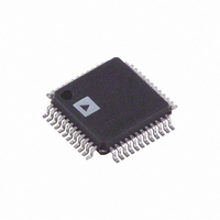
ADUC7032BSTZ-8V-RL Analog Devices Inc, ADUC7032BSTZ-8V-RL Datasheet - Page 24

ADUC7032BSTZ-8V-RL
Manufacturer Part Number
ADUC7032BSTZ-8V-RL
Description
IC BATTERY SENSOR PREC 48-LQFP
Manufacturer
Analog Devices Inc
Series
MicroConverter® ADuC7xxxr
Datasheet
1.ADUC7032BSTZ-8V-RL.pdf
(128 pages)
Specifications of ADUC7032BSTZ-8V-RL
Core Processor
ARM7
Core Size
16/32-Bit
Speed
20.48MHz
Connectivity
LIN, SPI, UART/USART
Peripherals
POR, PSM, Temp Sensor, WDT
Number Of I /o
9
Program Memory Size
96KB (96K x 8)
Program Memory Type
FLASH
Ram Size
6K x 8
Voltage - Supply (vcc/vdd)
3.5 V ~ 18 V
Data Converters
A/D 2x16b
Oscillator Type
Internal
Operating Temperature
-40°C ~ 105°C
Package / Case
48-LQFP
Lead Free Status / RoHS Status
Lead free / RoHS Compliant
Eeprom Size
-
Other names
ADUC7032BSTZ-8V-RLCT
Available stocks
Company
Part Number
Manufacturer
Quantity
Price
Company:
Part Number:
ADUC7032BSTZ-8V-RL
Manufacturer:
Analog Devices Inc
Quantity:
10 000
Preliminary Technical Data
Pin#
13
14
15
16
17
18
19
20
21
22
23
24
25
26
27
28
29
30
31
32
Mnemonic
VBAT
VREF
GND_SW
NC
NC
VTEMP
IIN+
IIN-
AGND
AGND
NC
REG_AVDD
NC
NC
GPIO_0/IRQ0/SS
GPIO_1/SCLK
GPIO_2/MIS0
GPIO_3/MOSI
GPIO_4/ECLK
NC
Type
I/O
I/O
I/O
I/O
I/O
S
S
S
S
I
I
I
I
I
*
Rev. PrD | Page 24 of 128
Function
Battery Voltage Input to resistor divider
External Reference Input Terminal. If this input is not being used it should be
connected directly to the AGND system ground
Switch to internal analog ground reference.
Negative input for external temperature channel and external reference
If this input is not being used it should be connected directly to the AGND
system ground.
No Connect, this pin is not connected internally but is reserved for possible
future use, this pin should therefore not be connected externally
No Connect, this pin is not connected internally but is reserved for possible
future use, this pin should therefore not be connected externally
External Pin for NTC/PTC temperature measurement
Positive Differential Input for Current Channel
Negative Differential Input for Current Channel
Ground Reference for On-Chip Precision Analog Circuits
Ground Reference for On-Chip Precision Analog Circuits
No Connect, this pin is not connected internally but is reserved for possible
future use, this pin should therefore not be connected externally
Nominal 2.6V output from on chip regulator
No Connect, this pin is not connected internally but is reserved for possible
future use, this pin should therefore not be connected externally
No Connect, this pin is not connected internally but is reserved for possible
future use, this pin should therefore not be connected externally
General Purpose Digital I/O 0 is a Multi-Function Pin. By default and after
Power-On-Reset, this pin is configured as an input. The pin has an internal
weak pull-up resistor and if not being used it can be left unconnected. This
multi-function pin can be configured in one of 3 states, namely:
General Purpose Digital I/O 0
External Interrupt Request 0, Active High
SPI Interface, Slave Select Input
General Purpose Digital I/O 1 is a Multi-Function Pin. By default and after
Power-On-Reset, this pin is configured as an input. The pin has an internal
weak pull-up resistor and if not being used it can be left unconnected. This
multi-function pin can be configured in one of 2 states, namely:
General Purpose Digital I/O 1
SPI Interface, Serial Clock Input
General Purpose Digital I/O 2 is a Multi-Function Pin. By default and after
Power-On-Reset, this pin is configured as an input. The pin has an internal
weak pull-up resistor and if not being used it can be left unconnected. This
multi-function pin can be configured in one of 2 states, namely:
General Purpose Digital I/O 2
SPI Interface, Master Input/Slave Output Pin
General Purpose Digital I/O 3 is a Multi-Function Pin. By default and after
Power-On-Reset, this pin is configured as an input. The pin has an internal
weak pull-up resistor and if not being used it can be left unconnected. This
multi-function pin can be configured in one of 2 states, namely:
General Purpose Digital I/O 3
SPI Interface, Master Output/Slave Input Pin
General Purpose Digital I/O 4 is a programmable digital I/O pin. By default and
after Power-On-Reset, this pin is configured as an input. The pin has an
internal weak pull-up resistor and if not being used this pin can be left
unconnected.
GPIO4 is can also be configured to output a 2.56MHz clock
No Connect, this pin is not connected internally but is reserved for possible
future use, this pin should therefore not be connected externally
ADuC7032


