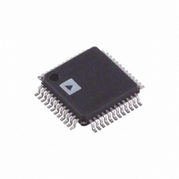
ADUC7032BSTZ-8V-RL Analog Devices Inc, ADUC7032BSTZ-8V-RL Datasheet - Page 31

ADUC7032BSTZ-8V-RL
Manufacturer Part Number
ADUC7032BSTZ-8V-RL
Description
IC BATTERY SENSOR PREC 48-LQFP
Manufacturer
Analog Devices Inc
Series
MicroConverter® ADuC7xxxr
Datasheet
1.ADUC7032BSTZ-8V-RL.pdf
(128 pages)
Specifications of ADUC7032BSTZ-8V-RL
Core Processor
ARM7
Core Size
16/32-Bit
Speed
20.48MHz
Connectivity
LIN, SPI, UART/USART
Peripherals
POR, PSM, Temp Sensor, WDT
Number Of I /o
9
Program Memory Size
96KB (96K x 8)
Program Memory Type
FLASH
Ram Size
6K x 8
Voltage - Supply (vcc/vdd)
3.5 V ~ 18 V
Data Converters
A/D 2x16b
Oscillator Type
Internal
Operating Temperature
-40°C ~ 105°C
Package / Case
48-LQFP
Lead Free Status / RoHS Status
Lead free / RoHS Compliant
Eeprom Size
-
Other names
ADUC7032BSTZ-8V-RLCT
Available stocks
Company
Part Number
Manufacturer
Quantity
Price
Company:
Part Number:
ADUC7032BSTZ-8V-RL
Manufacturer:
Analog Devices Inc
Quantity:
10 000
Preliminary Technical Data
FLASH/EE MEMORY AND THE ADUC7032
The ADuC7032 incorporates Flash/EE memory technology on-
chip to provide the user with non-volatile, in-circuit
reprogrammable memory space.
Like EEPROM, Flash memory can be programmed in-system at
a byte level, although it must first be erased, the erase being
performed in page blocks. Thus, Flash memory is often and
more correctly referred to as Flash/EE memory.
Overall, Flash/EE memory represents a step closer to the ideal
memory
programmability, high density, and low cost. Incorporated in
the ADuC7032 Flash/EE memory technology allows the user to
update program code space in-circuit, without the need to
replace one time programmable (OTP) devices at remote
operating nodes.
Flash/EE Memory
The total 96kBytes of Flash/EE memory are organized as 48k X
16 bits. 94kBytes are user space and 2kBytes are reserved for
boot loader/kernel space. The page size of this Flash/EE
memory is 512Bytes. Typically, it takes the Flash/EE memory
controller 20msec to erase a page, and 50µsec to write a 16-Bit
word. These Flash/EE memory timings are independent of
MCU core clock.
94kBytes of Flash/EE memory are available to the user as code
and non-volatile data memory. There is no distinction between
data and program, as ARM code shares the same space. The real
width of the Flash/EE memory is 16 bits, which means that in
ARM mode (32-bit instruction), two accesses to the Flash/EE
memory are necessary for each instruction fetch. When
operating at speeds less than 20.48MHz the Flash/EE memory
controller can transparently fetch the second 16-bit half word
(part of the 32-bit ARM op-code) within a single core clock
period. It is therefore recommend that for speeds less than
20.48MHz, i.e. CD > 0, that ARM mode is used. For 20.48MHz
operation, i.e. CD = 0 , it is recommended to operate in
THUMB mode.
The Flash/EE memory is physically located at 0x80000. Upon a
hard reset it is logically mapped to 0x00000000. The factory
default contents of all Flash/EE memory locations is 0xFF.
Flash/EE memory may be read in 8/16/32 bit segments, and
written in segments of 16 bits. The Flash/EE memory is rated
for 10K endurance cycles. This rating is based on the number of
times that each individual half word ( 16 bit location ) is cycled
i.e. erased and programmed. A redundancy scheme may be
implemented in software to ensure greater than 10K cycles
endurance.
The user may also write data variables to the Flash/EE memory
during run-time code execution, e.g. for storing diagnostic
device that
includes
non-volatility,
in-circuit
Rev. PrD | Page 31 of 128
battery parameter data.
It is possible to write to a single 16 bit location only twice
between erases, i.e. It is possible to walk bytes, not bits. If a
location is written to more than twice, then it is possible that
the contents of the Flash/EE page may be corrupted.
The 94kBytes of Flash/EE memory can be programmed in-
circuit, using a serial download mode via the LIN interface or
the integrated JTAG port.
The ADuC7032 facilitates code download via the LIN pin.
(2) JTAG access
The ADuC7032 features an on-chip JTAG Debug Port to
facilitate code download and debug.
FLASH/EE MEMORY CONTROL INTERFACE
The access to and control of the Flash/EE memory on the
ADuC7032 is managed by an on-chip memory controller. The
controller manages the Flash/EE memory as two separate
blocks (0 and 1).
Block 0 consists of the 32KB Flash/EE memory mapped from
0x0009 0000 to 0x0009 7FFF (including the 2KB kernel space
which is reserved at the top of this block).
Block 1 consists of the 64KB Flash/EE memory mapped from
from 0x0008 0000 to 0x0008 FFFF.
It should be noted that MCU core can continue to execute code
from one memory block while an active erase or program cycle
is being carried out on the other block. If a command operates
on the same block as the code currently executing, the core is
halted until the command is completed, this also applies to code
execution.
User Code, LIN and JTAG programming use the Flash/EE
memory Control Interface, which consists of the following
MMRs :
- FEExSTA (x= 0 or 1): read only register, reflects the status of
- FEExMOD (x= 0 or 1): sets the operating mode of the Flash
- FEExCON (x= 0 or 1): 8-bit command register. The
- FEExDAT (x= 0 or 1): 16-bit data register.
- FEExADR (x= 0 or 1): 16-bit address register.
- FEExSIGN (x= 0 or 1): Holds the 24-bit code signature as a
- FEExHIDE (x= 0 or 1): Protection MMR. Controls read and
(1) Serial Downloading (In-Circuit Programming)
the Flash Control Interface
Control Interface
commands are interpreted as described in Table 11.
result of the signature command being initiated.
write protection of the Flash memory code space. If
previously configured via the FEEPRO register, FEEHIDE
may require a software key to enable access.
ADuC7032


