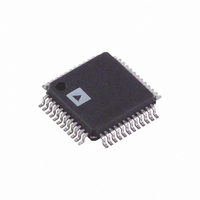
ADUC7032BSTZ-8V-RL Analog Devices Inc, ADUC7032BSTZ-8V-RL Datasheet - Page 64

ADUC7032BSTZ-8V-RL
Manufacturer Part Number
ADUC7032BSTZ-8V-RL
Description
IC BATTERY SENSOR PREC 48-LQFP
Manufacturer
Analog Devices Inc
Series
MicroConverter® ADuC7xxxr
Datasheet
1.ADUC7032BSTZ-8V-RL.pdf
(128 pages)
Specifications of ADUC7032BSTZ-8V-RL
Core Processor
ARM7
Core Size
16/32-Bit
Speed
20.48MHz
Connectivity
LIN, SPI, UART/USART
Peripherals
POR, PSM, Temp Sensor, WDT
Number Of I /o
9
Program Memory Size
96KB (96K x 8)
Program Memory Type
FLASH
Ram Size
6K x 8
Voltage - Supply (vcc/vdd)
3.5 V ~ 18 V
Data Converters
A/D 2x16b
Oscillator Type
Internal
Operating Temperature
-40°C ~ 105°C
Package / Case
48-LQFP
Lead Free Status / RoHS Status
Lead free / RoHS Compliant
Eeprom Size
-
Other names
ADUC7032BSTZ-8V-RLCT
Available stocks
Company
Part Number
Manufacturer
Quantity
Price
Company:
Part Number:
ADUC7032BSTZ-8V-RL
Manufacturer:
Analog Devices Inc
Quantity:
10 000
Preliminary Technical Data
ADC Calibration
As described in detail in the top level diagrams at the start of
this section, the signal flow through all ADC Channels can be
described in simple terms as:
Each ADC has a specific Offset and Gain correction or
Calibration coefficient associated with it that are stored in
MMR based Offset and Gain registers(ADCxOF and
ADCxGN). The offset and gain registers can be used to remove
offsets and gain errors arising within the part as well as System-
level offset and gain errors external to the part.
These registers are configured at power-on with a factory
programmed calibration value. These factory calibration values
will vary from part to part reflecting the manufacturing
variability of internal ADC circuits . However, these registers
can also be overwritten by user code (only if the ADC is in idle
mode) and will be automatically overwritten if an offset or gain
calibration cycle is initiated by user via the mode bits in the
ADCMDE[2:0] MMR. 2 types of automatic calibration are
available to the user, namely :
- Self (Offset or Gain) Calibration, where the ADC
generates its calibration coefficient based on an
internally generated 0V in the case of Self-Offset
calibration and full-scale voltage in the case of Self-Gain
calibration. It should be emphasized that ADC Self-
Calibrations correct for offset and gain errors within the
ADC. Self calibrations cannot compensate for other
external errors in the system, e.g. Shunt-Resistor
tolerance/drift, external offset voltages etc.
- System (Offset or Gain) Calibration, where the ADC
generates its calibration coefficient based on an
externally generated zero-scale voltage in the case of
System-Offset calibration and Full-scale voltage in the
case of System-Gain calibration which are applied to the
external ADC input for the duration of the calibration
cycle.
An Input-voltage is applied through an input buffer
(and PGA in the case of the I-ADC) to the Sigma-
Delta Modulator.
The Modulator-output is applied to a programmable
Digital Decimation Filter
The filter output result is then averaged if chopping is
used.
An Offset value (ADCxOF) is subtracted from the
result.
This result is scaled by a Gain value (ADCxGN).
Finally, the result is formatted as
- 2’s Complement. / Offset-Binary,
- Rounded to 16-Bit
- Clamped to +/-Full-Scale
Rev. PrD | Page 64 of 128
The duration of an Offset calibration is 1 single conversion
cycle (3/F
ADC to idle mode. A Gain calibration is a 2 stage process and
subsequently takes twice as long as an offset calibration cycle.
Once a calibration cycle is initiated, any ongoing ADC
conversion is immediately halted, the calibration is carried out
automatically at an ADC update rate programmed into
ADCFLT and the ADC is always returned to idle after any
calibration cycle. It is strongly recommended that ADC
calibration is initiated at as low an ADC update rate as possible
(high SF value in ADCFLT) in order to minimize the impact of
ADC noise during calibration.
NOTE: ADC0OF and ADC0GN must first contain the values
for PGA = 1 before a calibration scheme is started
Using the Offset and Gain Calibration Registers
If the Chop bit (ADCFLT[15]) is enabled, then internal ADC
offset errors will be minimized and an Offset calibration may
not be required. If chopping is disabled however, an initial
Offset calibration will be required and may need to be repeated.
A Gain calibration, particularly in the context of the I-ADC
(with internal PGA) may need to be carried out at all relevant
system gain ranges depending on system accuracy
requirements. If it is not possible to apply an external full-scale
current on all gain ranges then it is possible to apply a lower
current, and scale the result produced by the calibration. e.g
Apply a 50% current and then divide the ADC0GN value
produced by 2 and write this value back into ADC0GN. It
should be noted that there is a lower limit to the input signal
that can be applied for a System-Calibration because the
ADC0GN register is only 16-Bit. The input span (difference
between the System Zero-Scale value and System Full-Scale
value) should be greater than 40% of the nominal Full-Scale-
Input range, ie > 40% of Vref/Gain.
The on-chip Flash/EE memory can be used to store multiple
calibration coefficients which can be copied by user code
directly into the relevant calibration registers as appropriate
based on system configuration. In general, the simplest way to
use the calibration registers is to let the ADC calculate the
values required as part of the ADC automatic calibration
modes.
ADC
Chop off, 2/F
ADC
Chop on) before returning the
ADuC7032


