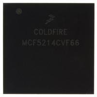
MCF5214CVF66 Freescale Semiconductor, MCF5214CVF66 Datasheet - Page 238

MCF5214CVF66
Manufacturer Part Number
MCF5214CVF66
Description
IC MPU 32BIT COLDF 256-MAPBGA
Manufacturer
Freescale Semiconductor
Series
MCF521xr
Datasheet
1.MCF5216CVM66J.pdf
(766 pages)
Specifications of MCF5214CVF66
Core Processor
Coldfire V2
Core Size
32-Bit
Speed
66MHz
Connectivity
CAN, EBI/EMI, I²C, SPI, UART/USART
Peripherals
DMA, LVD, POR, PWM, WDT
Number Of I /o
142
Program Memory Size
256KB (256K x 8)
Program Memory Type
FLASH
Ram Size
64K x 8
Voltage - Supply (vcc/vdd)
2.7 V ~ 3.6 V
Data Converters
A/D 8x12b
Oscillator Type
Internal
Operating Temperature
-40°C ~ 85°C
Package / Case
256-MAPBGA
Package
256MA-BGA
Device Core
ColdFire
Family Name
MCF521x
Maximum Speed
66 MHz
Operating Supply Voltage
3.3 V
Data Bus Width
32 Bit
Number Of Programmable I/os
142
Interface Type
QSPI/UART/I2C/CAN
On-chip Adc
8-chx10-bit
Number Of Timers
8
Lead Free Status / RoHS Status
Contains lead / RoHS non-compliant
Eeprom Size
-
Available stocks
Company
Part Number
Manufacturer
Quantity
Price
Company:
Part Number:
MCF5214CVF66
Manufacturer:
Freescale Semiconductor
Quantity:
10 000
Company:
Part Number:
MCF5214CVF66J
Manufacturer:
Freescale Semiconductor
Quantity:
10 000
- Current page: 238 of 766
- Download datasheet (9Mb)
External Interface Module (EIM)
13.5
Because operands can reside at any byte boundary, unlike opcodes, they are allowed to be misaligned. A
byte operand is properly aligned at any address, a word operand is misaligned at an odd address, and a
longword is misaligned at an address not a multiple of four. Although the processor enforces no alignment
restrictions for data operands (including program counter (PC) relative data addressing), additional bus
cycles are required for misaligned operands.
Instruction words and extension words (opcodes) must reside on word boundaries. Attempting to prefetch
a misaligned instruction word causes an address error exception.
The processor converts misaligned, cache-inhibited operand accesses to multiple aligned accesses.
Figure 13-19
example, SIZ[1:0] specify a byte transfer and a byte offset of 0x1. The slave device supplies the byte and
acknowledges the data transfer. When the processor starts the second cycle, SIZ[1:0] specify a word
transfer with a byte offset of 0x2. The next two bytes are transferred in this cycle. In the third cycle, byte
3 is transferred. The byte offset is now 0x0, the port supplies the final byte, and the operation is complete.
If an operand is cacheable and is misaligned across a cache-line boundary, both lines are loaded into the
cache. The example in
the transfer takes only two bus cycles.
13-14
CLKOUT
R/W, TIP
OE, BSn
SIZ[1:0]
D[31:0]
A[31:0]
CSn
TS
TA
Misaligned Operands
Transfer 1
Transfer 2
Transfer 3
shows the transfer of a longword operand from a byte address to a 32-bit port. In this
Figure 13-19. Example of a Misaligned Longword Transfer (32-Bit Port)
31
S0
Figure 13-20
MCF5282 and MCF5216 ColdFire Microcontroller User’s Manual, Rev. 3
S1
Byte 3
—
—
A[3:2] = 00
S2 S3 S4 S5 S0 S1 S4 S5 S0 S1 S4 S5 S0 S1 S4 S5
Basic
Write
Line
Figure 13-18. Line Write Burst-Inhibited
24 23
differs from that in
Byte 0
—
—
A[3:2] = 01
16 15
Fast
Write
Figure 13-19
Byte 1
—
—
A[3:2] = 10
Longword
8 7
Fast
in that the operand is word-sized and
Write
Byte 2
—
—
A[3:2] = 11
0
Fast
Freescale Semiconductor
Write
A[2:0]
001
010
100
Related parts for MCF5214CVF66
Image
Part Number
Description
Manufacturer
Datasheet
Request
R
Part Number:
Description:
Manufacturer:
Freescale Semiconductor, Inc
Datasheet:
Part Number:
Description:
Manufacturer:
Freescale Semiconductor, Inc
Datasheet:
Part Number:
Description:
Manufacturer:
Freescale Semiconductor, Inc
Datasheet:
Part Number:
Description:
Manufacturer:
Freescale Semiconductor, Inc
Datasheet:
Part Number:
Description:
Manufacturer:
Freescale Semiconductor, Inc
Datasheet:
Part Number:
Description:
Manufacturer:
Freescale Semiconductor, Inc
Datasheet:
Part Number:
Description:
Manufacturer:
Freescale Semiconductor, Inc
Datasheet:
Part Number:
Description:
Manufacturer:
Freescale Semiconductor, Inc
Datasheet:
Part Number:
Description:
Manufacturer:
Freescale Semiconductor, Inc
Datasheet:
Part Number:
Description:
Manufacturer:
Freescale Semiconductor, Inc
Datasheet:
Part Number:
Description:
Manufacturer:
Freescale Semiconductor, Inc
Datasheet:
Part Number:
Description:
Manufacturer:
Freescale Semiconductor, Inc
Datasheet:
Part Number:
Description:
Manufacturer:
Freescale Semiconductor, Inc
Datasheet:
Part Number:
Description:
Manufacturer:
Freescale Semiconductor, Inc
Datasheet:
Part Number:
Description:
Manufacturer:
Freescale Semiconductor, Inc
Datasheet:


