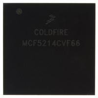
MCF5214CVF66 Freescale Semiconductor, MCF5214CVF66 Datasheet - Page 672

MCF5214CVF66
Manufacturer Part Number
MCF5214CVF66
Description
IC MPU 32BIT COLDF 256-MAPBGA
Manufacturer
Freescale Semiconductor
Series
MCF521xr
Datasheet
1.MCF5216CVM66J.pdf
(766 pages)
Specifications of MCF5214CVF66
Core Processor
Coldfire V2
Core Size
32-Bit
Speed
66MHz
Connectivity
CAN, EBI/EMI, I²C, SPI, UART/USART
Peripherals
DMA, LVD, POR, PWM, WDT
Number Of I /o
142
Program Memory Size
256KB (256K x 8)
Program Memory Type
FLASH
Ram Size
64K x 8
Voltage - Supply (vcc/vdd)
2.7 V ~ 3.6 V
Data Converters
A/D 8x12b
Oscillator Type
Internal
Operating Temperature
-40°C ~ 85°C
Package / Case
256-MAPBGA
Package
256MA-BGA
Device Core
ColdFire
Family Name
MCF521x
Maximum Speed
66 MHz
Operating Supply Voltage
3.3 V
Data Bus Width
32 Bit
Number Of Programmable I/os
142
Interface Type
QSPI/UART/I2C/CAN
On-chip Adc
8-chx10-bit
Number Of Timers
8
Lead Free Status / RoHS Status
Contains lead / RoHS non-compliant
Eeprom Size
-
Available stocks
Company
Part Number
Manufacturer
Quantity
Price
Company:
Part Number:
MCF5214CVF66
Manufacturer:
Freescale Semiconductor
Quantity:
10 000
Company:
Part Number:
MCF5214CVF66J
Manufacturer:
Freescale Semiconductor
Quantity:
10 000
- Current page: 672 of 766
- Download datasheet (9Mb)
IEEE 1149.1 Test Access Port (JTAG)
31.5.3.4 TEST_LEAKAGE Instruction
The TEST_LEAKAGE instruction forces the jtag_leakage output signal to high. It is intended to tri-state
all output pad buffers and disable all of the part’s pad input buffers except TEST and TRST. The
jtag_leakage signal is asserted at the rising edge of TCLK when the TAP controller transitions from
update-IR to run-test/idle state. Once asserted, the part disables the TCLK, TMS, and TDI inputs into
JTAG and forces these JTAG inputs to logic 1. The TAP controller remains in the run-test/idle state until
the TRST input is asserted (logic 0).
31.5.3.5 ENABLE_TEST_CTRL Instruction
The ENABLE_TEST_CTRL instruction selects a 3-bit shift register (TEST_CTRL) for connection as a
shift path between the TDI and TDO pin. When the user transitions the TAP controller to the UPDATE_DR
state, the register transfers its value to a parallel hold register. It allows the control chip to test functions
independent of the JTAG TAP controller state.
31.5.3.6 HIGHZ Instruction
The HIGHZ instruction eliminates the need to backdrive the output pins during circuit-board testing.
HIGHZ turns off all output drivers, including the 2-state drivers, and selects the bypass register. HIGHZ
also asserts internal reset for the MCU system logic to force a predictable internal state.
31.5.3.7 LOCKOUT_RECOVERY Instruction
If a user inadvertently enables security on a MCU, the LOCKOUT_RECOVERY instruction allows the
disabling of security by the complete erasure of the internal flash contents including the configuration
field. This does not compromise security as the entire contents of the user’s secured code stored in flash
gets erased before security is disabled on the MCU on the next reset or power-up sequence.
The LOCKOUT_RECOVERY instruction selects a 7-bit shift register for connection as a shift path
between the TDI pin and the TDO pin. When the user transitions the TAP controller to the UPDATE-DR
state, the 7-bit shift register is loaded into the 7-bit JTAG_TFM_CLKDIV register and this value is output
to the TFM’s clock divider circuit. When the user transitions the TAP controller to the RUN-TEST/IDLE
state, the erase signal to the TFM asserts and the lockout sequence starts. The controller must remain in
that state until the erase sequence has completed. Once the lockout recovery sequence has completed, the
user must reset both the JTAG TAP controller and the MCU to return to normal operation.
31-8
•
accessible by shifting it through the boundary scan register to the TDO output by using the
shift-DR state. Both the data capture and the shift operation are transparent to system operation.
PRELOAD - initialize the boundary scan register update cells before selecting EXTEST or
CLAMP. This is achieved by ignoring the data shifting out on the TDO pin and shifting in
initialization data. The update-DR state and the falling edge of TCLK can then transfer this data to
the update cells. The data is applied to the external output pins by the EXTEST or CLAMP
instruction.
External synchronization is required to achieve meaningful results because
there is no internal synchronization between TCLK and the system clock.
MCF5282 and MCF5216 ColdFire Microcontroller User’s Manual, Rev. 3
NOTE
Freescale Semiconductor
Related parts for MCF5214CVF66
Image
Part Number
Description
Manufacturer
Datasheet
Request
R
Part Number:
Description:
Manufacturer:
Freescale Semiconductor, Inc
Datasheet:
Part Number:
Description:
Manufacturer:
Freescale Semiconductor, Inc
Datasheet:
Part Number:
Description:
Manufacturer:
Freescale Semiconductor, Inc
Datasheet:
Part Number:
Description:
Manufacturer:
Freescale Semiconductor, Inc
Datasheet:
Part Number:
Description:
Manufacturer:
Freescale Semiconductor, Inc
Datasheet:
Part Number:
Description:
Manufacturer:
Freescale Semiconductor, Inc
Datasheet:
Part Number:
Description:
Manufacturer:
Freescale Semiconductor, Inc
Datasheet:
Part Number:
Description:
Manufacturer:
Freescale Semiconductor, Inc
Datasheet:
Part Number:
Description:
Manufacturer:
Freescale Semiconductor, Inc
Datasheet:
Part Number:
Description:
Manufacturer:
Freescale Semiconductor, Inc
Datasheet:
Part Number:
Description:
Manufacturer:
Freescale Semiconductor, Inc
Datasheet:
Part Number:
Description:
Manufacturer:
Freescale Semiconductor, Inc
Datasheet:
Part Number:
Description:
Manufacturer:
Freescale Semiconductor, Inc
Datasheet:
Part Number:
Description:
Manufacturer:
Freescale Semiconductor, Inc
Datasheet:
Part Number:
Description:
Manufacturer:
Freescale Semiconductor, Inc
Datasheet:


