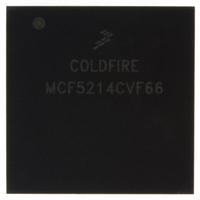
MCF5214CVF66 Freescale Semiconductor, MCF5214CVF66 Datasheet - Page 571

MCF5214CVF66
Manufacturer Part Number
MCF5214CVF66
Description
IC MPU 32BIT COLDF 256-MAPBGA
Manufacturer
Freescale Semiconductor
Series
MCF521xr
Datasheet
1.MCF5216CVM66J.pdf
(766 pages)
Specifications of MCF5214CVF66
Core Processor
Coldfire V2
Core Size
32-Bit
Speed
66MHz
Connectivity
CAN, EBI/EMI, I²C, SPI, UART/USART
Peripherals
DMA, LVD, POR, PWM, WDT
Number Of I /o
142
Program Memory Size
256KB (256K x 8)
Program Memory Type
FLASH
Ram Size
64K x 8
Voltage - Supply (vcc/vdd)
2.7 V ~ 3.6 V
Data Converters
A/D 8x12b
Oscillator Type
Internal
Operating Temperature
-40°C ~ 85°C
Package / Case
256-MAPBGA
Package
256MA-BGA
Device Core
ColdFire
Family Name
MCF521x
Maximum Speed
66 MHz
Operating Supply Voltage
3.3 V
Data Bus Width
32 Bit
Number Of Programmable I/os
142
Interface Type
QSPI/UART/I2C/CAN
On-chip Adc
8-chx10-bit
Number Of Timers
8
Lead Free Status / RoHS Status
Contains lead / RoHS non-compliant
Eeprom Size
-
Available stocks
Company
Part Number
Manufacturer
Quantity
Price
Company:
Part Number:
MCF5214CVF66
Manufacturer:
Freescale Semiconductor
Quantity:
10 000
Company:
Part Number:
MCF5214CVF66J
Manufacturer:
Freescale Semiconductor
Quantity:
10 000
- Current page: 571 of 766
- Download datasheet (9Mb)
If the amplifier bypass mode is enabled for a conversion by setting the amplifier bypass (BYP) field in the
CCW, the timing changes to that shown in
Table (CCW)
potential conversion time by two QCLKs. When using the bypass mode, the external circuit should be of
low source impedance (typically less than 10 kΩ). Also, the loading effects on the external circuitry of the
QADC need to be considered, because the benefits of the sample amplifier are not present.
28.7.3.3 Channel Decode and Multiplexer
The internal multiplexer selects one of the eight analog input signals for conversion. The selected input is
connected to the sample buffer amplifier or to the sample capacitor. The multiplexer also includes positive
and negative stress protection circuitry, which prevents deselected channels from affecting the selected
channel when current is injected into the deselected channels.
28.7.3.4 Sample Buffer
The sample buffer is used to raise the effective input impedance of the A/D converter, so that external
factors (higher bandwidth or higher impedance) are less critical to accuracy. The input voltage is buffered
onto the sample capacitor to reduce crosstalk between channels.
28.7.3.5 Comparator
The comparator output feeds into the SAR, which accumulates the A/D conversion result sequentially,
beginning with the MSB.
Freescale Semiconductor
QCLK
for more information on the BYP field. The initial sample time is eliminated, reducing the
QCLK
Because of internal RC time constants, use of a two QCLK sample time in
bypass mode will cause serious errors when operating the QADC at high
frequencies.
2 Cycles
Sample
Sample Time
Buffer
Time:
n CYCLES
(2,4,8,16)
Sample
MCF5282 and MCF5216 ColdFire Microcontroller User’s Manual, Rev. 3
Sample Time
Time:
Figure 28-21. Bypass Mode Conversion Timing
(2,4,8,16)
n Cycles
Sample
Time:
Final
Figure 28-20. Conversion Timing
Successive Approximation Resolution Sequence
Figure
Successive Approximation Resolution Sequence
28-21. See
NOTE
Resolution
10 Cycles
Time:
Resolution
10 Cycles
Section 28.6.7, “Conversion Command Word
Time:
Queued Analog-to-Digital Converter (QADC)
28-33
Related parts for MCF5214CVF66
Image
Part Number
Description
Manufacturer
Datasheet
Request
R
Part Number:
Description:
Manufacturer:
Freescale Semiconductor, Inc
Datasheet:
Part Number:
Description:
Manufacturer:
Freescale Semiconductor, Inc
Datasheet:
Part Number:
Description:
Manufacturer:
Freescale Semiconductor, Inc
Datasheet:
Part Number:
Description:
Manufacturer:
Freescale Semiconductor, Inc
Datasheet:
Part Number:
Description:
Manufacturer:
Freescale Semiconductor, Inc
Datasheet:
Part Number:
Description:
Manufacturer:
Freescale Semiconductor, Inc
Datasheet:
Part Number:
Description:
Manufacturer:
Freescale Semiconductor, Inc
Datasheet:
Part Number:
Description:
Manufacturer:
Freescale Semiconductor, Inc
Datasheet:
Part Number:
Description:
Manufacturer:
Freescale Semiconductor, Inc
Datasheet:
Part Number:
Description:
Manufacturer:
Freescale Semiconductor, Inc
Datasheet:
Part Number:
Description:
Manufacturer:
Freescale Semiconductor, Inc
Datasheet:
Part Number:
Description:
Manufacturer:
Freescale Semiconductor, Inc
Datasheet:
Part Number:
Description:
Manufacturer:
Freescale Semiconductor, Inc
Datasheet:
Part Number:
Description:
Manufacturer:
Freescale Semiconductor, Inc
Datasheet:
Part Number:
Description:
Manufacturer:
Freescale Semiconductor, Inc
Datasheet:


