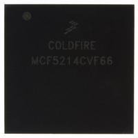
MCF5214CVF66 Freescale Semiconductor, MCF5214CVF66 Datasheet - Page 40

MCF5214CVF66
Manufacturer Part Number
MCF5214CVF66
Description
IC MPU 32BIT COLDF 256-MAPBGA
Manufacturer
Freescale Semiconductor
Series
MCF521xr
Datasheet
1.MCF5216CVM66J.pdf
(766 pages)
Specifications of MCF5214CVF66
Core Processor
Coldfire V2
Core Size
32-Bit
Speed
66MHz
Connectivity
CAN, EBI/EMI, I²C, SPI, UART/USART
Peripherals
DMA, LVD, POR, PWM, WDT
Number Of I /o
142
Program Memory Size
256KB (256K x 8)
Program Memory Type
FLASH
Ram Size
64K x 8
Voltage - Supply (vcc/vdd)
2.7 V ~ 3.6 V
Data Converters
A/D 8x12b
Oscillator Type
Internal
Operating Temperature
-40°C ~ 85°C
Package / Case
256-MAPBGA
Package
256MA-BGA
Device Core
ColdFire
Family Name
MCF521x
Maximum Speed
66 MHz
Operating Supply Voltage
3.3 V
Data Bus Width
32 Bit
Number Of Programmable I/os
142
Interface Type
QSPI/UART/I2C/CAN
On-chip Adc
8-chx10-bit
Number Of Timers
8
Lead Free Status / RoHS Status
Contains lead / RoHS non-compliant
Eeprom Size
-
Available stocks
Company
Part Number
Manufacturer
Quantity
Price
Company:
Part Number:
MCF5214CVF66
Manufacturer:
Freescale Semiconductor
Quantity:
10 000
Company:
Part Number:
MCF5214CVF66J
Manufacturer:
Freescale Semiconductor
Quantity:
10 000
- Current page: 40 of 766
- Download datasheet (9Mb)
Overview
The SRAM module is also accessible by non-core bus masters, for example the DMA and/or the FEC. The
dual-ported nature of the SRAM makes it ideal for implementing applications with double-buffer schemes,
where the processor and a DMA device operate in alternate regions of the SRAM to maximize system
performance. As an example, system performance can be increased significantly if Ethernet packets are
moved from the FEC into the SRAM (rather than external memory) prior to any processing.
1.1.1.3
This product incorporates SuperFlash® technology licensed from SST. The ColdFire Flash Module (CFM)
is a non-volatile memory (NVM) module for integration with the processor core. The CFM is constructed
with eight banks of 32K x 16-bit Flash arrays to generate 512 Kbytes of 32-bit Flash memory
These arrays serve as electrically erasable and programmable, non-volatile program and data memory. The
Flash memory is ideal for program and data storage for single-chip applications allowing for field
reprogramming without requiring an external programming voltage source. The CFM interfaces to the
V2 ColdFire core through an optimized read-only memory controller which supports interleaved accesses
from the 2-cycle Flash arrays. A “backdoor” mapping of the Flash memory is used for all program, erase,
and verify operations. It also provides a read datapath for non-core masters (for example, DMA).
1.1.1.4
The ColdFire processor core debug interface is provided to support system debugging in conjunction with
low-cost debug and emulator development tools. Through a standard debug interface, users can access
real-time trace and debug information. This allows the processor and system to be debugged at full speed
without the need for costly in-circuit emulators. The debug interface is a superset of the BDM interface
provided on Freescale’s 683xx family of parts.
The on-chip breakpoint resources include a total of 6 programmable registers—a set of address registers
(with two 32-bit registers), a set of data registers (with a 32-bit data register plus a 32-bit data mask
register), and one 32-bit PC register plus a 32-bit PC mask register. These registers can be accessed through
the dedicated debug serial communication channel or from the processor’s supervisor mode programming
model. The breakpoint registers can be configured to generate triggers by combining the address, data, and
PC conditions in a variety of single or dual-level definitions. The trigger event can be programmed to
generate a processor halt or initiate a debug interrupt exception.
To support program trace, the Version 2 debug module provides processor status (PST[3:0]) and debug
data (DDATA[3:0]) ports. These buses and the CLKOUT output provide execution status, captured
operand data, and branch target addresses defining the dynamic execution path of the processor at the
CPU’s clock rate.
1.1.2
This section details the functionality of the System Control Module (SCM) which provides the
programming model for the System Access Control Unit (SACU), the system bus arbiter, a 32-bit Core
Watchdog Timer (CWT), and the system control registers and logic. Specifically, the system control
includes the internal peripheral system base address register (IPSBAR), the processor’s dual-port RAM
1-8
System Control Module
Flash
Debug Module
The CFM on the MCF5281 and MCF5214 is constructed with four banks of
32K x 16-bit Flash arrays to generate 256 Kbytes of 32-bit Flash memory.
The MCF5280 does not contain a CFM.
MCF5282 and MCF5216 ColdFire Microcontroller User’s Manual, Rev. 3
NOTE
Freescale Semiconductor
Related parts for MCF5214CVF66
Image
Part Number
Description
Manufacturer
Datasheet
Request
R
Part Number:
Description:
Manufacturer:
Freescale Semiconductor, Inc
Datasheet:
Part Number:
Description:
Manufacturer:
Freescale Semiconductor, Inc
Datasheet:
Part Number:
Description:
Manufacturer:
Freescale Semiconductor, Inc
Datasheet:
Part Number:
Description:
Manufacturer:
Freescale Semiconductor, Inc
Datasheet:
Part Number:
Description:
Manufacturer:
Freescale Semiconductor, Inc
Datasheet:
Part Number:
Description:
Manufacturer:
Freescale Semiconductor, Inc
Datasheet:
Part Number:
Description:
Manufacturer:
Freescale Semiconductor, Inc
Datasheet:
Part Number:
Description:
Manufacturer:
Freescale Semiconductor, Inc
Datasheet:
Part Number:
Description:
Manufacturer:
Freescale Semiconductor, Inc
Datasheet:
Part Number:
Description:
Manufacturer:
Freescale Semiconductor, Inc
Datasheet:
Part Number:
Description:
Manufacturer:
Freescale Semiconductor, Inc
Datasheet:
Part Number:
Description:
Manufacturer:
Freescale Semiconductor, Inc
Datasheet:
Part Number:
Description:
Manufacturer:
Freescale Semiconductor, Inc
Datasheet:
Part Number:
Description:
Manufacturer:
Freescale Semiconductor, Inc
Datasheet:
Part Number:
Description:
Manufacturer:
Freescale Semiconductor, Inc
Datasheet:


