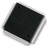
S912XEQ384J3CAL Freescale Semiconductor, S912XEQ384J3CAL Datasheet - Page 1027

S912XEQ384J3CAL
Manufacturer Part Number
S912XEQ384J3CAL
Description
IC MCU 16BIT 384KB FLASH 112LQFP
Manufacturer
Freescale Semiconductor
Series
HCS12r
Datasheet
1.S912XEQ384J3CAL.pdf
(1328 pages)
Specifications of S912XEQ384J3CAL
Core Processor
HCS12X
Core Size
16-Bit
Speed
50MHz
Connectivity
CAN, EBI/EMI, I²C, IrDA, SCI, SPI
Peripherals
LVD, POR, PWM, WDT
Number Of I /o
91
Program Memory Size
384KB (384K x 8)
Program Memory Type
FLASH
Eeprom Size
4K x 8
Ram Size
24K x 8
Voltage - Supply (vcc/vdd)
1.72 V ~ 5.5 V
Data Converters
A/D 16x12b
Oscillator Type
External
Operating Temperature
-40°C ~ 85°C
Package / Case
112-LQFP
Core
HCS12X
Data Bus Width
16 bit
Data Ram Size
24 KB
Interface Type
SCI, SPI, I2C, CAN
Maximum Clock Frequency
50 MHz
Number Of Programmable I/os
91
Number Of Timers
1
Operating Supply Voltage
3.13 V to 5.5 V
Maximum Operating Temperature
+ 260 C
Mounting Style
SMD/SMT
Lead Free Status / RoHS Status
Lead free / RoHS Compliant
Available stocks
Company
Part Number
Manufacturer
Quantity
Price
Company:
Part Number:
S912XEQ384J3CAL
Manufacturer:
Freescale Semiconductor
Quantity:
10 000
- Current page: 1027 of 1328
- Download datasheet (9Mb)
27.3.2
The Flash module contains a set of 20 control and status registers located between Flash module base +
0x0000 and 0x0013. A summary of the Flash module registers is given in
descriptions in the following subsections.
Freescale Semiconductor
FERCNFG
FCCOBIX
FECCRIX
FCLKDIV
Address
& Name
FCNFG
0x0000
0x0001
0x0002
0x0003
0x0004
0x0005
FSEC
1. Duplicate value used if primary value generates a double bit fault when read during the reset sequence.
0x12_0000 – 0x12_0001
0x12_0002 – 0x12_0003
0x12_0004 – 0x12_0005
0x12_0006 – 0x12_0007
0x12_0008 – 0x12_007F
Global Address
(EEEIFRON)
Register Descriptions
W
W
W
W
W
W
R
R
R
R
R
R
Writes to any Flash register must be avoided while a Flash command is
active (CCIF=0) to prevent corruption of Flash register contents and
Memory Controller behavior.
ERSERIE
KEYEN1
FDIVLD
CCIE
7
0
0
Table 27-7. EEE Nonvolatile Information Register Fields
PGMERIE
KEYEN0
(Bytes)
FDIV6
MC9S12XE-Family Reference Manual , Rev. 1.23
Figure 27-4. FTM512K3 Register Summary
Size
120
6
0
0
0
2
2
2
2
D-Flash User Partition (DFPART)
Refer to
D-Flash User Partition (duplicate
Buffer RAM EEE Partition (ERPART)
Refer to
Buffer RAM EEE Partition (duplicate
Reserved
FDIV5
RNV5
5
0
0
0
0
Section 27.4.2.15, “Full Partition D-Flash
Section 27.4.2.15, “Full Partition D-Flash
CAUTION
EPVIOLIE
IGNSF
FDIV4
RNV4
4
0
0
Chapter 27 512 KByte Flash Module (S12XFTM512K3V1)
ERSVIE1
FDIV3
RNV3
Description
3
0
0
0
(1)
)
1
)
CCOBIX2
ECCRIX2
ERSVIE0
Figure 27-4
FDIV2
RNV2
2
0
Command”
Command”
CCOBIX1
ECCRIX1
DFDIE
FDIV1
FDFD
SEC1
with detailed
1
CCOBIX0
ECCRIX0
FDIV0
SFDIE
SEC0
FSFD
0
1027
Related parts for S912XEQ384J3CAL
Image
Part Number
Description
Manufacturer
Datasheet
Request
R
Part Number:
Description:
Manufacturer:
Freescale Semiconductor, Inc
Datasheet:
Part Number:
Description:
Manufacturer:
Freescale Semiconductor, Inc
Datasheet:
Part Number:
Description:
Manufacturer:
Freescale Semiconductor, Inc
Datasheet:
Part Number:
Description:
Manufacturer:
Freescale Semiconductor, Inc
Datasheet:
Part Number:
Description:
Manufacturer:
Freescale Semiconductor, Inc
Datasheet:
Part Number:
Description:
Manufacturer:
Freescale Semiconductor, Inc
Datasheet:
Part Number:
Description:
Manufacturer:
Freescale Semiconductor, Inc
Datasheet:
Part Number:
Description:
Manufacturer:
Freescale Semiconductor, Inc
Datasheet:
Part Number:
Description:
Manufacturer:
Freescale Semiconductor, Inc
Datasheet:
Part Number:
Description:
Manufacturer:
Freescale Semiconductor, Inc
Datasheet:
Part Number:
Description:
Manufacturer:
Freescale Semiconductor, Inc
Datasheet:
Part Number:
Description:
Manufacturer:
Freescale Semiconductor, Inc
Datasheet:
Part Number:
Description:
Manufacturer:
Freescale Semiconductor, Inc
Datasheet:
Part Number:
Description:
Manufacturer:
Freescale Semiconductor, Inc
Datasheet:
Part Number:
Description:
Manufacturer:
Freescale Semiconductor, Inc
Datasheet:


