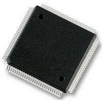
S912XEQ384J3CAL Freescale Semiconductor, S912XEQ384J3CAL Datasheet - Page 143

S912XEQ384J3CAL
Manufacturer Part Number
S912XEQ384J3CAL
Description
IC MCU 16BIT 384KB FLASH 112LQFP
Manufacturer
Freescale Semiconductor
Series
HCS12r
Datasheet
1.S912XEQ384J3CAL.pdf
(1328 pages)
Specifications of S912XEQ384J3CAL
Core Processor
HCS12X
Core Size
16-Bit
Speed
50MHz
Connectivity
CAN, EBI/EMI, I²C, IrDA, SCI, SPI
Peripherals
LVD, POR, PWM, WDT
Number Of I /o
91
Program Memory Size
384KB (384K x 8)
Program Memory Type
FLASH
Eeprom Size
4K x 8
Ram Size
24K x 8
Voltage - Supply (vcc/vdd)
1.72 V ~ 5.5 V
Data Converters
A/D 16x12b
Oscillator Type
External
Operating Temperature
-40°C ~ 85°C
Package / Case
112-LQFP
Core
HCS12X
Data Bus Width
16 bit
Data Ram Size
24 KB
Interface Type
SCI, SPI, I2C, CAN
Maximum Clock Frequency
50 MHz
Number Of Programmable I/os
91
Number Of Timers
1
Operating Supply Voltage
3.13 V to 5.5 V
Maximum Operating Temperature
+ 260 C
Mounting Style
SMD/SMT
Lead Free Status / RoHS Status
Lead free / RoHS Compliant
Available stocks
Company
Part Number
Manufacturer
Quantity
Price
Company:
Part Number:
S912XEQ384J3CAL
Manufacturer:
Freescale Semiconductor
Quantity:
10 000
- Current page: 143 of 1328
- Download datasheet (9Mb)
1. Read: Anytime.
2.3.47
Freescale Semiconductor
Address 0x025A
Write: Anytime.
DDRP
DDRP
Field
Field
PTIP
Reset
7-0
6-0
7
W
R
Port P input data—
This register always reads back the buffered state of the associated pins. This can also be used to detect overload
or short circuit conditions on output pins.
Port P data direction—
This register controls the data direction of pin 7.
The enabled PWM channel 7 forces the I/O state to be an output. If the PWM shutdown feature is enabled this pin
is forced to be an input. In these cases the data direction bit will not change.
1 Associated pin is configured as output.
0 Associated pin is configured as input.
Port P data direction—
The PWM forces the I/O state to be an output for each port line associated with an enabled PWM6-0 channel. In this
case the data direction bit will not change.
1 Associated pin is configured as output.
0 Associated pin is configured as input.
DDRP7
Port P Data Direction Register (DDRP)
0
7
Due to internal synchronization circuits, it can take up to 2 bus clock cycles
until the correct value is read on PTP or PTIP registers, when changing the
DDRP register.
DDRP6
0
6
Figure 2-45. Port P Data Direction Register (DDRP)
Table 2-43. DDRP Register Field Descriptions
Table 2-42. PTIP Register Field Descriptions
MC9S12XE-Family Reference Manual , Rev. 1.23
DDRP5
0
5
DDRP4
NOTE
0
4
Description
Description
DDRP3
3
0
Chapter 2 Port Integration Module (S12XEPIMV1)
DDRP2
0
2
Access: User read/write
DDRP1
0
1
DDRP0
0
0
143
(1)
Related parts for S912XEQ384J3CAL
Image
Part Number
Description
Manufacturer
Datasheet
Request
R
Part Number:
Description:
Manufacturer:
Freescale Semiconductor, Inc
Datasheet:
Part Number:
Description:
Manufacturer:
Freescale Semiconductor, Inc
Datasheet:
Part Number:
Description:
Manufacturer:
Freescale Semiconductor, Inc
Datasheet:
Part Number:
Description:
Manufacturer:
Freescale Semiconductor, Inc
Datasheet:
Part Number:
Description:
Manufacturer:
Freescale Semiconductor, Inc
Datasheet:
Part Number:
Description:
Manufacturer:
Freescale Semiconductor, Inc
Datasheet:
Part Number:
Description:
Manufacturer:
Freescale Semiconductor, Inc
Datasheet:
Part Number:
Description:
Manufacturer:
Freescale Semiconductor, Inc
Datasheet:
Part Number:
Description:
Manufacturer:
Freescale Semiconductor, Inc
Datasheet:
Part Number:
Description:
Manufacturer:
Freescale Semiconductor, Inc
Datasheet:
Part Number:
Description:
Manufacturer:
Freescale Semiconductor, Inc
Datasheet:
Part Number:
Description:
Manufacturer:
Freescale Semiconductor, Inc
Datasheet:
Part Number:
Description:
Manufacturer:
Freescale Semiconductor, Inc
Datasheet:
Part Number:
Description:
Manufacturer:
Freescale Semiconductor, Inc
Datasheet:
Part Number:
Description:
Manufacturer:
Freescale Semiconductor, Inc
Datasheet:


