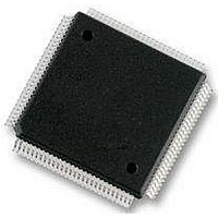
S912XEQ384J3CAL Freescale Semiconductor, S912XEQ384J3CAL Datasheet - Page 93

S912XEQ384J3CAL
Manufacturer Part Number
S912XEQ384J3CAL
Description
IC MCU 16BIT 384KB FLASH 112LQFP
Manufacturer
Freescale Semiconductor
Series
HCS12r
Datasheet
1.S912XEQ384J3CAL.pdf
(1328 pages)
Specifications of S912XEQ384J3CAL
Core Processor
HCS12X
Core Size
16-Bit
Speed
50MHz
Connectivity
CAN, EBI/EMI, I²C, IrDA, SCI, SPI
Peripherals
LVD, POR, PWM, WDT
Number Of I /o
91
Program Memory Size
384KB (384K x 8)
Program Memory Type
FLASH
Eeprom Size
4K x 8
Ram Size
24K x 8
Voltage - Supply (vcc/vdd)
1.72 V ~ 5.5 V
Data Converters
A/D 16x12b
Oscillator Type
External
Operating Temperature
-40°C ~ 85°C
Package / Case
112-LQFP
Core
HCS12X
Data Bus Width
16 bit
Data Ram Size
24 KB
Interface Type
SCI, SPI, I2C, CAN
Maximum Clock Frequency
50 MHz
Number Of Programmable I/os
91
Number Of Timers
1
Operating Supply Voltage
3.13 V to 5.5 V
Maximum Operating Temperature
+ 260 C
Mounting Style
SMD/SMT
Lead Free Status / RoHS Status
Lead free / RoHS Compliant
Available stocks
Company
Part Number
Manufacturer
Quantity
Price
Company:
Part Number:
S912XEQ384J3CAL
Manufacturer:
Freescale Semiconductor
Quantity:
10 000
- Current page: 93 of 1328
- Download datasheet (9Mb)
Chapter 2
Port Integration Module (S12XEPIMV1)
2.1
2.1.1
The S12XE Family Port Integration Module establishes the interface between the peripheral modules
including the non-multiplexed External Bus Interface module (S12X_EBI) and the I/O pins for all ports.
It controls the electrical pin properties as well as the signal prioritization and multiplexing on shared pins.
This document covers:
Freescale Semiconductor
Revision
Number
V01.17
V01.18
V01.19
•
•
•
•
•
•
•
•
•
•
•
•
•
Port A and B used as address output of the S12X_EBI
Port C and D used as data I/O of the S12X_EBI
Port E associated with the S12X_EBI control signals and the IRQ, XIRQ interrupt inputs
Port K associated with address output and control signals of the S12X_EBI
Port T associated with 1 ECT module
Port S associated with 2 SCI and 1 SPI modules
Port M associated with 4 MSCAN and 1 SCI module
Port P connected to the PWM and 2 SPI modules - inputs can be used as an external interrupt source
Port H associated with 4 SCI modules - inputs can be used as an external interrupt source
Port J associated with 1 MSCAN, 1 SCI, 2 IIC modules and chip select outputs - inputs can be used
as an external interrupt source
Port AD0 and AD1 associated with two 16-channel ATD modules
Port R associated with 1 standard timer (TIM) module
Port L associated with 4 SCI modules
Introduction
Overview
Revision Date
25 Nov 2008
18 Dec 2009
02 Apr 2008
2.4.3.4/185
2.3.19/124
MC9S12XE-Family Reference Manual , Rev. 1.23
Sections
Affected
Table 2-1. Revision History
• Corrected reduced drive strength to 1/5
• Separated PE1,0 bit descriptions from other PE GPIO
• Corrected alternative functions on Port K (ACC[2:0])
• Corrected functions on PE[5] (MODB) and PE[2] (WE)
• Added function independency to reduced drive and wired-or bit
• Minor corrections
descriptions
Description of Changes
93
Related parts for S912XEQ384J3CAL
Image
Part Number
Description
Manufacturer
Datasheet
Request
R
Part Number:
Description:
Manufacturer:
Freescale Semiconductor, Inc
Datasheet:
Part Number:
Description:
Manufacturer:
Freescale Semiconductor, Inc
Datasheet:
Part Number:
Description:
Manufacturer:
Freescale Semiconductor, Inc
Datasheet:
Part Number:
Description:
Manufacturer:
Freescale Semiconductor, Inc
Datasheet:
Part Number:
Description:
Manufacturer:
Freescale Semiconductor, Inc
Datasheet:
Part Number:
Description:
Manufacturer:
Freescale Semiconductor, Inc
Datasheet:
Part Number:
Description:
Manufacturer:
Freescale Semiconductor, Inc
Datasheet:
Part Number:
Description:
Manufacturer:
Freescale Semiconductor, Inc
Datasheet:
Part Number:
Description:
Manufacturer:
Freescale Semiconductor, Inc
Datasheet:
Part Number:
Description:
Manufacturer:
Freescale Semiconductor, Inc
Datasheet:
Part Number:
Description:
Manufacturer:
Freescale Semiconductor, Inc
Datasheet:
Part Number:
Description:
Manufacturer:
Freescale Semiconductor, Inc
Datasheet:
Part Number:
Description:
Manufacturer:
Freescale Semiconductor, Inc
Datasheet:
Part Number:
Description:
Manufacturer:
Freescale Semiconductor, Inc
Datasheet:
Part Number:
Description:
Manufacturer:
Freescale Semiconductor, Inc
Datasheet:


