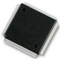
S912XEQ384J3CAL Freescale Semiconductor, S912XEQ384J3CAL Datasheet - Page 830

S912XEQ384J3CAL
Manufacturer Part Number
S912XEQ384J3CAL
Description
IC MCU 16BIT 384KB FLASH 112LQFP
Manufacturer
Freescale Semiconductor
Series
HCS12r
Datasheet
1.S912XEQ384J3CAL.pdf
(1328 pages)
Specifications of S912XEQ384J3CAL
Core Processor
HCS12X
Core Size
16-Bit
Speed
50MHz
Connectivity
CAN, EBI/EMI, I²C, IrDA, SCI, SPI
Peripherals
LVD, POR, PWM, WDT
Number Of I /o
91
Program Memory Size
384KB (384K x 8)
Program Memory Type
FLASH
Eeprom Size
4K x 8
Ram Size
24K x 8
Voltage - Supply (vcc/vdd)
1.72 V ~ 5.5 V
Data Converters
A/D 16x12b
Oscillator Type
External
Operating Temperature
-40°C ~ 85°C
Package / Case
112-LQFP
Core
HCS12X
Data Bus Width
16 bit
Data Ram Size
24 KB
Interface Type
SCI, SPI, I2C, CAN
Maximum Clock Frequency
50 MHz
Number Of Programmable I/os
91
Number Of Timers
1
Operating Supply Voltage
3.13 V to 5.5 V
Maximum Operating Temperature
+ 260 C
Mounting Style
SMD/SMT
Lead Free Status / RoHS Status
Lead free / RoHS Compliant
Available stocks
Company
Part Number
Manufacturer
Quantity
Price
Company:
Part Number:
S912XEQ384J3CAL
Manufacturer:
Freescale Semiconductor
Quantity:
10 000
- Current page: 830 of 1328
- Download datasheet (9Mb)
Chapter 23 Voltage Regulator (S12VREGL3V3V1)
The API Trimming bits APITR[5:0] must be set so the minimum period equals 0.2 ms if stable frequency
is desired.
See
It is possible to generate with the API a waveform at an external pin by enabling the API by setting APIFE
and enabling the external access with setting APIEA. By setting APIES the waveform can be selected. If
APIES is set, then at the external pin a clock is visible with 2 times the selected API Period
If APIES is not set, then at the external pin will be a high pulse at the end of every selected period with the
size of half of the min period
23.4.9
This section describes how VREG_3V3 controls the reset of the MCU.The reset values of registers and
signals are provided in
listed in
23.4.10 Description of Reset Operation
23.4.10.1 Power-On Reset (POR)
During chip power-up the digital core may not work if its supply voltage V
deassertion level (V
is kept high until V
The power-on reset is active in all operation modes of VREG_3V3.
23.4.10.2 Low-Voltage Reset (LVR)
For details on low-voltage reset, see
23.4.11 Interrupts
This section describes all interrupts originated by VREG_3V3.
The interrupt vectors requested by VREG_3V3 are listed in
priorities are defined at MCU level.
830
Because of an order from the United States International Trade Commission, BGA-packaged product lines and partnumbers
indicated here currently are not available from Freescale for import or sale in the United States prior to September 2010
Table 23-7
Table
Resets
23-12.
The first period after enabling the counter by APIFE might be reduced by
API start up delay t
if VREG_3V3 is in Shutdown Mode.
for the trimming effect of APITR.
DD
PORD
exceeds V
Section 23.3, “Memory Map and Register
). Therefore, signal POR, which forces the other blocks of the device into reset,
Low-voltage reset
Power-on reset
Reset Source
(Table
MC9S12XE-Family Reference Manual , Rev. 1.23
PORD
sdel
23-9). See device level specification for connectivity.
Section 23.4.5, “Low-Voltage Reset
. The API internal RC oscillator clock is not available
. The MCU will run the start-up sequence after POR deassertion.
Table 23-12. Reset Sources
Available only in Full Performance Mode
NOTE
Local Enable
Always active
Table
Definition”. Possible reset sources are
23-13. Vector addresses and interrupt
(LVR)”.
DD
is below the POR
Freescale Semiconductor
(Table
23-9).
Related parts for S912XEQ384J3CAL
Image
Part Number
Description
Manufacturer
Datasheet
Request
R
Part Number:
Description:
Manufacturer:
Freescale Semiconductor, Inc
Datasheet:
Part Number:
Description:
Manufacturer:
Freescale Semiconductor, Inc
Datasheet:
Part Number:
Description:
Manufacturer:
Freescale Semiconductor, Inc
Datasheet:
Part Number:
Description:
Manufacturer:
Freescale Semiconductor, Inc
Datasheet:
Part Number:
Description:
Manufacturer:
Freescale Semiconductor, Inc
Datasheet:
Part Number:
Description:
Manufacturer:
Freescale Semiconductor, Inc
Datasheet:
Part Number:
Description:
Manufacturer:
Freescale Semiconductor, Inc
Datasheet:
Part Number:
Description:
Manufacturer:
Freescale Semiconductor, Inc
Datasheet:
Part Number:
Description:
Manufacturer:
Freescale Semiconductor, Inc
Datasheet:
Part Number:
Description:
Manufacturer:
Freescale Semiconductor, Inc
Datasheet:
Part Number:
Description:
Manufacturer:
Freescale Semiconductor, Inc
Datasheet:
Part Number:
Description:
Manufacturer:
Freescale Semiconductor, Inc
Datasheet:
Part Number:
Description:
Manufacturer:
Freescale Semiconductor, Inc
Datasheet:
Part Number:
Description:
Manufacturer:
Freescale Semiconductor, Inc
Datasheet:
Part Number:
Description:
Manufacturer:
Freescale Semiconductor, Inc
Datasheet:


