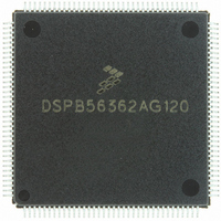
DSPB56362AG120 Freescale Semiconductor, DSPB56362AG120 Datasheet - Page 11

DSPB56362AG120
Manufacturer Part Number
DSPB56362AG120
Description
IC DSP 24BIT AUD 120MHZ 144-LQFP
Manufacturer
Freescale Semiconductor
Series
Symphony™r
Type
Audio Processorr
Datasheet
1.DSPB56362AG120.pdf
(152 pages)
Specifications of DSPB56362AG120
Interface
Host Interface, I²C, SAI, SPI
Clock Rate
120MHz
Non-volatile Memory
ROM (126 kB)
On-chip Ram
42kB
Voltage - I/o
3.30V
Voltage - Core
3.30V
Operating Temperature
-40°C ~ 85°C
Mounting Type
Surface Mount
Package / Case
144-LQFP
Device Core Size
24b
Architecture
Modified Harvard
Format
Fixed Point
Clock Freq (max)
120MHz
Mips
120
Device Input Clock Speed
120MHz
Ram Size
42KB
Program Memory Size
90KB
Operating Supply Voltage (typ)
3.3V
Operating Supply Voltage (min)
3.14V
Operating Supply Voltage (max)
3.46V
Operating Temp Range
-40C to 105C
Operating Temperature Classification
Industrial
Mounting
Surface Mount
Pin Count
144
Package Type
LQFP
Product
DSPs
Data Bus Width
24 bit
Processor Series
DSP563xx
Core
56000
Numeric And Arithmetic Format
Fixed-Point
Instruction Set Architecture
Modified Harvard
Device Million Instructions Per Second
120 MIPS
Maximum Clock Frequency
120 MHz
Program Memory Type
Flash
Data Ram Size
42 KB
Operating Supply Voltage
3.3 V
Maximum Operating Temperature
+ 105 C
Mounting Style
SMD/SMT
Interface Type
SPI, I2C, ESAI, SHI
Minimum Operating Temperature
- 40 C
Lead Free Status / RoHS Status
Lead free / RoHS Compliant
Available stocks
Company
Part Number
Manufacturer
Quantity
Price
Company:
Part Number:
DSPB56362AG120
Manufacturer:
FSC
Quantity:
12 000
Company:
Part Number:
DSPB56362AG120
Manufacturer:
FREESCA
Quantity:
273
Company:
Part Number:
DSPB56362AG120
Manufacturer:
Freescale Semiconductor
Quantity:
10 000
Part Number:
DSPB56362AG120
Manufacturer:
N/A
Quantity:
20 000
2.5
When the DSP56362 enters a low-power standby mode (stop or wait), it releases bus mastership and
tri-states the relevant port A signals: A0–A17, D0–D23, AA0/RAS0–AA3/RAS3, RD, WR, BB, CAS.
2.5.1
2.5.2
Freescale Semiconductor
Signal Name
Signal Name
Signal Name
PINIT/NMI
D0–D23
PCAP
A0–A17
External Memory Expansion Port (Port A)
External Address Bus
External Data Bus
Type
Input
Input
Input/Output
Output
Type
Type
State during Reset
Input
Input
State during Reset
State during Reset
Table 2-4 Clock and PLL Signals (continued)
Table 2-5 External Address Bus Signals
Tri-Stated
Tri-Stated
Table 2-6 External Data Bus Signals
DSP56362 Technical Data, Rev. 4
PLL Capacitor—PCAP is an input connecting an off-chip capacitor to the PLL
filter. Connect one capacitor terminal to PCAP and the other terminal to V
If the PLL is not used, PCAP may be tied to V
PLL Initial/Non maskable Interrupt—During assertion of RESET, the value of
PINIT/NMI is written into the PLL Enable (PEN) bit of the PLL control register,
determining whether the PLL is enabled or disabled. After RESET deassertion
and during normal instruction processing, the PINIT/NMI Schmitt-trigger input
is a negative-edge-triggered non maskable interrupt (NMI) request internally
synchronized to CLKOUT.
PINIT/NMI cannot tolerate 5 V.
Data Bus—When the DSP is the bus master, D0–D23 are active-high,
bidirectional input/outputs that provide the bidirectional data bus for
external program and data memory accesses. Otherwise, D0–D23 are
tri-stated.
Address Bus—When the DSP is the bus master, A0–A17 are
active-high outputs that specify the address for external program and
data memory accesses. Otherwise, the signals are tri-stated. To
minimize power dissipation, A0–A17 do not change state when
external memory spaces are not being accessed.
Signal Description
Signal Description
Signal Description
External Memory Expansion Port (Port A)
CC
, GND, or left floating.
CCP
2-5
.


