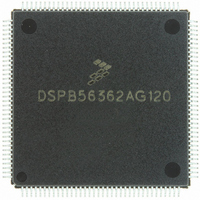
DSPB56362AG120 Freescale Semiconductor, DSPB56362AG120 Datasheet - Page 113

DSPB56362AG120
Manufacturer Part Number
DSPB56362AG120
Description
IC DSP 24BIT AUD 120MHZ 144-LQFP
Manufacturer
Freescale Semiconductor
Series
Symphony™r
Type
Audio Processorr
Datasheet
1.DSPB56362AG120.pdf
(152 pages)
Specifications of DSPB56362AG120
Interface
Host Interface, I²C, SAI, SPI
Clock Rate
120MHz
Non-volatile Memory
ROM (126 kB)
On-chip Ram
42kB
Voltage - I/o
3.30V
Voltage - Core
3.30V
Operating Temperature
-40°C ~ 85°C
Mounting Type
Surface Mount
Package / Case
144-LQFP
Device Core Size
24b
Architecture
Modified Harvard
Format
Fixed Point
Clock Freq (max)
120MHz
Mips
120
Device Input Clock Speed
120MHz
Ram Size
42KB
Program Memory Size
90KB
Operating Supply Voltage (typ)
3.3V
Operating Supply Voltage (min)
3.14V
Operating Supply Voltage (max)
3.46V
Operating Temp Range
-40C to 105C
Operating Temperature Classification
Industrial
Mounting
Surface Mount
Pin Count
144
Package Type
LQFP
Product
DSPs
Data Bus Width
24 bit
Processor Series
DSP563xx
Core
56000
Numeric And Arithmetic Format
Fixed-Point
Instruction Set Architecture
Modified Harvard
Device Million Instructions Per Second
120 MIPS
Maximum Clock Frequency
120 MHz
Program Memory Type
Flash
Data Ram Size
42 KB
Operating Supply Voltage
3.3 V
Maximum Operating Temperature
+ 105 C
Mounting Style
SMD/SMT
Interface Type
SPI, I2C, ESAI, SHI
Minimum Operating Temperature
- 40 C
Lead Free Status / RoHS Status
Lead free / RoHS Compliant
Available stocks
Company
Part Number
Manufacturer
Quantity
Price
Company:
Part Number:
DSPB56362AG120
Manufacturer:
FSC
Quantity:
12 000
Company:
Part Number:
DSPB56362AG120
Manufacturer:
FREESCA
Quantity:
273
Company:
Part Number:
DSPB56362AG120
Manufacturer:
Freescale Semiconductor
Quantity:
10 000
Part Number:
DSPB56362AG120
Manufacturer:
N/A
Quantity:
20 000
5.4.3
The frequency jitter of the PLL is defined as the variation of the frequency of CLKOUT. For small MF
(MF < 10) this jitter is smaller than 0.5%. For mid-range MF (10 < MF < 500) this jitter is between 0.5%
and approximately 2%. For large MF (MF > 500), the frequency jitter is 2–3%.
5.4.4
The allowed jitter on the frequency of EXTAL is 0.5%. If the rate of change of the frequency of EXTAL
is slow (i.e., it does not jump between the minimum and maximum values in one cycle) or the frequency
of the jitter is fast (i.e., it does not stay at an extreme value for a long time), then the allowed jitter can be
2%. The phase and frequency jitter performance results are only valid if the input jitter is less than the
prescribed values.
5.5
Careful synchronization is required when reading multi-bit registers that are written by another
asynchronous system. This synchronization is a common problem when two asynchronous systems are
connected, as they are in the host interface. The following paragraphs present considerations for proper
operation.
5.5.1
Freescale Semiconductor
•
•
•
Unsynchronized Reading of Receive Byte Registers—When reading the receive byte registers,
receive register high (RXH), receive register middle (RXM), or receive register low (RXL), the
host interface programmer should use interrupts or poll the receive register data full (RXDF) flag
that indicates whether data is available. This ensures that the data in the receive byte registers will
be valid.
Overwriting Transmit Byte Registers—The host interface programmer should not write to the
transmit byte registers, transmit register high (TXH), transmit register middle (TXM), or transmit
register low (TXL), unless the transmit register data empty (TXDE) bit is set, indicating that the
transmit byte registers are empty. This ensures that the transmit byte registers will transfer valid
data to the host receive (HRX) register.
Synchronization of Status Bits from DSP to Host—HC, HOREQ, DMA, HF3, HF2, TRDY,
TXDE, and RXDF status bits are set or cleared from inside the DSP and read by the host processor
(refer to the user’s manual for descriptions of these status bits). The host can read these status bits
very quickly without regard to the clock rate used by the DSP, but the state of the bit could be
changing during the read operation. This is not generally a system problem, because the bit will be read
correctly in the next pass of any host polling routine.
However, if the host asserts HEN for more than timing number 31, with
a minimum cycle time of timing number 31 + 32, then these status bits are guaranteed to be
stable. Exercise care when reading status bits HF3 and HF2 as an encoded pair. If the DSP
changes HF3 and HF2 from 00 to 11, there is a small probability that the host could read the bits
during the transition and receive 01 or 10 instead of 11. If the combination of HF3 and HF2 has
Host Port Considerations
Frequency Jitter Performance
Input (EXTAL) Jitter Requirements
Host Programming Considerations
DSP56362 Technical Data, Rev. 4
Host Port Considerations
5-5


