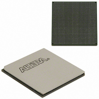
EP3SL150F1152C2N Altera, EP3SL150F1152C2N Datasheet - Page 100

EP3SL150F1152C2N
Manufacturer Part Number
EP3SL150F1152C2N
Description
IC STRATX III FPGA 150K 1152FBGA
Manufacturer
Altera
Series
Stratix® IIIr
Datasheets
1.EP3SL150F780C4N.pdf
(16 pages)
2.EP3SL150F780C4N.pdf
(332 pages)
3.EP3SL150F780C4N.pdf
(456 pages)
Specifications of EP3SL150F1152C2N
Number Of Logic Elements/cells
142500
Number Of Labs/clbs
5700
Total Ram Bits
6390
Number Of I /o
744
Voltage - Supply
0.86 V ~ 1.15 V
Mounting Type
Surface Mount
Operating Temperature
0°C ~ 85°C
Package / Case
1152-FBGA
For Use With
544-2568 - KIT DEVELOPMENT STRATIX III
Lead Free Status / RoHS Status
Lead free / RoHS Compliant
Number Of Gates
-
Other names
544-2409
EP3SL150F1152C2NES
EP3SL150F1152C2NES
Available stocks
Company
Part Number
Manufacturer
Quantity
Price
Part Number:
EP3SL150F1152C2N
Manufacturer:
ALTERA
Quantity:
20 000
- Current page: 100 of 456
- Download datasheet (7Mb)
4–20
Read/Write Clock Mode
Single Clock Mode
Design Considerations
Selecting TriMatrix Memory Blocks
Conflict Resolution
Stratix III Device Handbook, Volume 1
f
Stratix III TriMatrix memory blocks can implement read/write clock mode for simple
dual-port memories. In this mode, a write clock controls the data-input,
write-address, and write-enable registers. Similarly, a read clock control the
data-output, read-address, and read-enable registers. The memory blocks support
independent clock enables for both the read and write clocks. Asynchronous clears
are available on data output latches and registers only.
When using read/write mode, if you perform a simultaneous read/write to the same
address location, the output read data will be unknown. If you require the output data
to be a known value in this case, use either single-clock mode or input/output clock
mode and choose the appropriate read-during-write behavior in the Megawizard.
Stratix III TriMatrix memory blocks can implement single-clock mode for true
dual-port, simple dual-port, and single-port memories. In this mode, a single clock,
together with a clock enable, is used to control all registers of the memory block.
Asynchronous clears are available on output latches and output registers only.
This section describes guidelines for designing with TriMatrix memory blocks.
The Quartus II software automatically partitions user-defined memory into
embedded memory blocks by taking into account both speed and size constraints
placed on your design. For example, the Quartus II software may spread out a
memory across multiple memory blocks when resources are available to increase the
performance of the design. You can manually assign the memory to a specific block
size via the RAM MegaWizard Plug-In Manager.
MLABs can implement single-port SRAM through emulation via the Quartus II
software. Emulation results in minimal additional logic resources being used. Because
of the dual-purpose architecture of the MLAB, it only has data input registers and
output registers in the block. MLABs gain input address registers and additional
optional data output registers from adjacent ALMs by using register packing.
For more information about register packing, refer to the
Adaptive Logic Modules in Stratix III Devices
Handbook.
When using the memory blocks in true dual-port mode, it is possible to attempt two
write operations to the same memory location (address). Since no conflict resolution
circuitry is built into the memory blocks, this results in unknown data being written to
that location. Therefore, you must implement conflict resolution logic external to the
memory block to avoid address conflicts.
Chapter 4: TriMatrix Embedded Memory Blocks in Stratix III Devices
chapter in volume 1 of the Stratix III Device
Logic Array Blocks and
© May 2009 Altera Corporation
Design Considerations
Related parts for EP3SL150F1152C2N
Image
Part Number
Description
Manufacturer
Datasheet
Request
R

Part Number:
Description:
CYCLONE II STARTER KIT EP2C20N
Manufacturer:
Altera
Datasheet:

Part Number:
Description:
CPLD, EP610 Family, ECMOS Process, 300 Gates, 16 Macro Cells, 16 Reg., 16 User I/Os, 5V Supply, 35 Speed Grade, 24DIP
Manufacturer:
Altera Corporation
Datasheet:

Part Number:
Description:
CPLD, EP610 Family, ECMOS Process, 300 Gates, 16 Macro Cells, 16 Reg., 16 User I/Os, 5V Supply, 15 Speed Grade, 24DIP
Manufacturer:
Altera Corporation
Datasheet:

Part Number:
Description:
Manufacturer:
Altera Corporation
Datasheet:

Part Number:
Description:
CPLD, EP610 Family, ECMOS Process, 300 Gates, 16 Macro Cells, 16 Reg., 16 User I/Os, 5V Supply, 30 Speed Grade, 24DIP
Manufacturer:
Altera Corporation
Datasheet:

Part Number:
Description:
High-performance, low-power erasable programmable logic devices with 8 macrocells, 10ns
Manufacturer:
Altera Corporation
Datasheet:

Part Number:
Description:
High-performance, low-power erasable programmable logic devices with 8 macrocells, 7ns
Manufacturer:
Altera Corporation
Datasheet:

Part Number:
Description:
Classic EPLD
Manufacturer:
Altera Corporation
Datasheet:

Part Number:
Description:
High-performance, low-power erasable programmable logic devices with 8 macrocells, 10ns
Manufacturer:
Altera Corporation
Datasheet:

Part Number:
Description:
Manufacturer:
Altera Corporation
Datasheet:

Part Number:
Description:
Manufacturer:
Altera Corporation
Datasheet:

Part Number:
Description:
Manufacturer:
Altera Corporation
Datasheet:

Part Number:
Description:
CPLD, EP610 Family, ECMOS Process, 300 Gates, 16 Macro Cells, 16 Reg., 16 User I/Os, 5V Supply, 25 Speed Grade, 24DIP
Manufacturer:
Altera Corporation
Datasheet:


