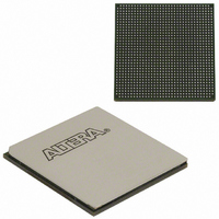
EP3SL150F1152C2N Altera, EP3SL150F1152C2N Datasheet - Page 252

EP3SL150F1152C2N
Manufacturer Part Number
EP3SL150F1152C2N
Description
IC STRATX III FPGA 150K 1152FBGA
Manufacturer
Altera
Series
Stratix® IIIr
Datasheets
1.EP3SL150F780C4N.pdf
(16 pages)
2.EP3SL150F780C4N.pdf
(332 pages)
3.EP3SL150F780C4N.pdf
(456 pages)
Specifications of EP3SL150F1152C2N
Number Of Logic Elements/cells
142500
Number Of Labs/clbs
5700
Total Ram Bits
6390
Number Of I /o
744
Voltage - Supply
0.86 V ~ 1.15 V
Mounting Type
Surface Mount
Operating Temperature
0°C ~ 85°C
Package / Case
1152-FBGA
For Use With
544-2568 - KIT DEVELOPMENT STRATIX III
Lead Free Status / RoHS Status
Lead free / RoHS Compliant
Number Of Gates
-
Other names
544-2409
EP3SL150F1152C2NES
EP3SL150F1152C2NES
Available stocks
Company
Part Number
Manufacturer
Quantity
Price
Part Number:
EP3SL150F1152C2N
Manufacturer:
ALTERA
Quantity:
20 000
- Current page: 252 of 456
- Download datasheet (7Mb)
8–4
Data and Data-Strobe/Clock Pins
Stratix III Device Handbook, Volume 1
f
1
1
1
Read data-strobes or clocks are called DQS pins. Depending on the memory
specifications, DQS pins can be bi-directional single-ended signals (in DDR2 and DDR
SDRAM), uni-directional differential signals (in RLDRAM II), bi-directional
differential signals (DDR3 and DDR2 SDRAM), or uni-directional complementary
signals (QDR II+ and QDR II SRAM). Connect the uni-directional read and write
data-strobes or clocks to Stratix III DQS pins.
Stratix III devices offer differential input buffers for differential read
data-strobe/clock operations and provide an independent DQS logic block for each
CQn pin for complementary read data-strobe/clock operations. The differential DQS
pin-pairs are denoted as DQS and DQSn pins, while the complementary DQS signals
are denoted as CQ and CQn pins. DQSn and CQn pins are marked separately in the
pin table. Each CQn pin connects to a DQS logic block and the shifted CQn signals go
to the negative-edge input registers in the IOE registers.
Use differential DQS signaling for DDR2 SDRAM interfaces running higher than
333 MHz.
For DDR3 and DDR2 SDRAM application, pseudo-differential DQS signaling is used
for write operation.
Stratix III DDR memory interface data pins are called DQ pins. DQ pins can be
bi-directional signals (in DDR3, DDR2, and DDR SDRAM, and RLDRAM II common
I/O (CIO) interfaces), or uni-directional signals (in QDR II+, QDR II SRAM, and
RLDRAM II separate I/O (SIO) devices). Connect the uni-directional read data signals
to Stratix III DQ pins and the uni-directional write data signals to a different DQS/DQ
group other than the read DQS/DQ group. You must assign the write clocks to the
DQS/DQSn pins associated to this write DQS/DQ group. Do not use the CQ/CQn
pin-pair for write clocks.
Using a DQS/DQ group for write data signals minimizes output skew, allows access
to the write leveling circuitry (for DDR3 SDRAM interfaces), and allows for vertical
migration. These pins also have access to deskewing circuitry that can compensate for
delay mismatch between signals on the bus.
For more information about pin planning, refer to
chapter in volume 2 of the External Memory Interface Handbook.
The DQS and DQ pin locations are fixed in the pin table. Memory interface circuitry is
available in every Stratix III I/O bank. All memory interface pins support the I/O
standards required to support DDR3, DDR2, DDR SDRAM, QDR II+, QDR II SRAM,
and RLDRAM II devices.
The Stratix III device supports DQS and DQ signals with DQ bus modes of ×4, ×8/×9,
×16/×18, or ×32/×36, although not all devices support DQS bus mode ×32/×36.
When any of these pins are not used for memory interfacing, you can use them as user
I/Os. In addition, you can use any DQSn or CQn pins not used for clocking as DQ
(data) pins.
DQS/CQ and DQSn/CQn pin pair.
Table 8–1
lists pin support per DQS/DQ bus mode, including the
Chapter 8: External Memory Interfaces in Stratix III Devices
Section I. Device and Pin Planning
© March 2010 Altera Corporation
Memory Interfaces Pin Support
Related parts for EP3SL150F1152C2N
Image
Part Number
Description
Manufacturer
Datasheet
Request
R

Part Number:
Description:
CYCLONE II STARTER KIT EP2C20N
Manufacturer:
Altera
Datasheet:

Part Number:
Description:
CPLD, EP610 Family, ECMOS Process, 300 Gates, 16 Macro Cells, 16 Reg., 16 User I/Os, 5V Supply, 35 Speed Grade, 24DIP
Manufacturer:
Altera Corporation
Datasheet:

Part Number:
Description:
CPLD, EP610 Family, ECMOS Process, 300 Gates, 16 Macro Cells, 16 Reg., 16 User I/Os, 5V Supply, 15 Speed Grade, 24DIP
Manufacturer:
Altera Corporation
Datasheet:

Part Number:
Description:
Manufacturer:
Altera Corporation
Datasheet:

Part Number:
Description:
CPLD, EP610 Family, ECMOS Process, 300 Gates, 16 Macro Cells, 16 Reg., 16 User I/Os, 5V Supply, 30 Speed Grade, 24DIP
Manufacturer:
Altera Corporation
Datasheet:

Part Number:
Description:
High-performance, low-power erasable programmable logic devices with 8 macrocells, 10ns
Manufacturer:
Altera Corporation
Datasheet:

Part Number:
Description:
High-performance, low-power erasable programmable logic devices with 8 macrocells, 7ns
Manufacturer:
Altera Corporation
Datasheet:

Part Number:
Description:
Classic EPLD
Manufacturer:
Altera Corporation
Datasheet:

Part Number:
Description:
High-performance, low-power erasable programmable logic devices with 8 macrocells, 10ns
Manufacturer:
Altera Corporation
Datasheet:

Part Number:
Description:
Manufacturer:
Altera Corporation
Datasheet:

Part Number:
Description:
Manufacturer:
Altera Corporation
Datasheet:

Part Number:
Description:
Manufacturer:
Altera Corporation
Datasheet:

Part Number:
Description:
CPLD, EP610 Family, ECMOS Process, 300 Gates, 16 Macro Cells, 16 Reg., 16 User I/Os, 5V Supply, 25 Speed Grade, 24DIP
Manufacturer:
Altera Corporation
Datasheet:


