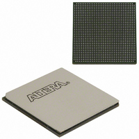
EP3SL150F1152C2N Altera, EP3SL150F1152C2N Datasheet - Page 222

EP3SL150F1152C2N
Manufacturer Part Number
EP3SL150F1152C2N
Description
IC STRATX III FPGA 150K 1152FBGA
Manufacturer
Altera
Series
Stratix® IIIr
Datasheets
1.EP3SL150F780C4N.pdf
(16 pages)
2.EP3SL150F780C4N.pdf
(332 pages)
3.EP3SL150F780C4N.pdf
(456 pages)
Specifications of EP3SL150F1152C2N
Number Of Logic Elements/cells
142500
Number Of Labs/clbs
5700
Total Ram Bits
6390
Number Of I /o
744
Voltage - Supply
0.86 V ~ 1.15 V
Mounting Type
Surface Mount
Operating Temperature
0°C ~ 85°C
Package / Case
1152-FBGA
For Use With
544-2568 - KIT DEVELOPMENT STRATIX III
Lead Free Status / RoHS Status
Lead free / RoHS Compliant
Number Of Gates
-
Other names
544-2409
EP3SL150F1152C2NES
EP3SL150F1152C2NES
Available stocks
Company
Part Number
Manufacturer
Quantity
Price
Part Number:
EP3SL150F1152C2N
Manufacturer:
ALTERA
Quantity:
20 000
- Current page: 222 of 456
- Download datasheet (7Mb)
7–18
Bus Hold
Programmable Pull-Up Resistor
Programmable Pre-Emphasis
Stratix III Device Handbook, Volume 1
f
f
1
Each Stratix III device I/O pin provides an optional bus-hold feature. The bus-hold
circuitry can weakly hold the signal on an I/O pin at its last-driven state. Because the
bus-hold feature holds the last-driven state of the pin until the next input signal is
present, you do not need an external pull-up or pull-down resistor to hold a signal
level when the bus is tri-stated.
The bus-hold circuitry also pulls non-driven pins away from the input threshold
voltage where noise can cause unintended high-frequency switching. You can select
this feature individually for each I/O pin. The bus-hold output drives no higher than
V
programmable pull-up option cannot be used. Disable the bus-hold feature if the I/O
pin is configured for differential signals.
The bus-hold circuitry uses a resistor with a nominal resistance (R
7 kΩ to weakly pull the signal level to the last-driven state.
For the specific sustaining current driven through this resistor and the overdrive
current used to identify the next-driven input level, refer to the
Characteristics of Stratix III Devices
voltage level.
The bus-hold circuitry is active only after configuration. When going into user mode,
the bus-hold circuit captures the value on the pin present at the end of configuration.
Each Stratix III device I/O pin provides an optional programmable pull-up resistor
during user mode. If you enable this feature for an I/O pin, the pull-up resistor
(typically 25 kΩ) weakly holds the I/O to the V
Programmable pull-up resistors are only supported on user I/O pins and are not
supported on dedicated configuration pins, JTAG pins, or dedicated clock pins. If the
programmable pull-up option is enabled, you cannot use the bus-hold feature.
When the optional DEV_OE signal drives low, all I/O pins remain tri-stated even with
programmable pull-up option enabled.
Stratix III LVDS transmitters support programmable pre-emphasis to compensate for
the frequency dependent attenuation of the transmission line. The Quartus II software
allows four settings for programmable pre-emphasis—zero, low, medium, and high.
The default setting is low.
For more information about programmable pre-emphasis, refer to the
Differential I/O Interfaces with DPA in the Stratix III Devices
CCIO
to prevent over-driving signals. If the bus-hold feature is enabled, the
chapter. This information is provided for each V
CCIO
level.
Chapter 7: Stratix III Device I/O Features
chapter.
© July 2010 Altera Corporation
DC and Switching
BH
) of approximately
Stratix III I/O Structure
High-Speed
CCIO
Related parts for EP3SL150F1152C2N
Image
Part Number
Description
Manufacturer
Datasheet
Request
R

Part Number:
Description:
CYCLONE II STARTER KIT EP2C20N
Manufacturer:
Altera
Datasheet:

Part Number:
Description:
CPLD, EP610 Family, ECMOS Process, 300 Gates, 16 Macro Cells, 16 Reg., 16 User I/Os, 5V Supply, 35 Speed Grade, 24DIP
Manufacturer:
Altera Corporation
Datasheet:

Part Number:
Description:
CPLD, EP610 Family, ECMOS Process, 300 Gates, 16 Macro Cells, 16 Reg., 16 User I/Os, 5V Supply, 15 Speed Grade, 24DIP
Manufacturer:
Altera Corporation
Datasheet:

Part Number:
Description:
Manufacturer:
Altera Corporation
Datasheet:

Part Number:
Description:
CPLD, EP610 Family, ECMOS Process, 300 Gates, 16 Macro Cells, 16 Reg., 16 User I/Os, 5V Supply, 30 Speed Grade, 24DIP
Manufacturer:
Altera Corporation
Datasheet:

Part Number:
Description:
High-performance, low-power erasable programmable logic devices with 8 macrocells, 10ns
Manufacturer:
Altera Corporation
Datasheet:

Part Number:
Description:
High-performance, low-power erasable programmable logic devices with 8 macrocells, 7ns
Manufacturer:
Altera Corporation
Datasheet:

Part Number:
Description:
Classic EPLD
Manufacturer:
Altera Corporation
Datasheet:

Part Number:
Description:
High-performance, low-power erasable programmable logic devices with 8 macrocells, 10ns
Manufacturer:
Altera Corporation
Datasheet:

Part Number:
Description:
Manufacturer:
Altera Corporation
Datasheet:

Part Number:
Description:
Manufacturer:
Altera Corporation
Datasheet:

Part Number:
Description:
Manufacturer:
Altera Corporation
Datasheet:

Part Number:
Description:
CPLD, EP610 Family, ECMOS Process, 300 Gates, 16 Macro Cells, 16 Reg., 16 User I/Os, 5V Supply, 25 Speed Grade, 24DIP
Manufacturer:
Altera Corporation
Datasheet:


