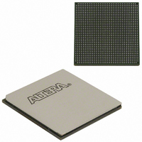
EP3SL150F1152C2N Altera, EP3SL150F1152C2N Datasheet - Page 278

EP3SL150F1152C2N
Manufacturer Part Number
EP3SL150F1152C2N
Description
IC STRATX III FPGA 150K 1152FBGA
Manufacturer
Altera
Series
Stratix® IIIr
Datasheets
1.EP3SL150F780C4N.pdf
(16 pages)
2.EP3SL150F780C4N.pdf
(332 pages)
3.EP3SL150F780C4N.pdf
(456 pages)
Specifications of EP3SL150F1152C2N
Number Of Logic Elements/cells
142500
Number Of Labs/clbs
5700
Total Ram Bits
6390
Number Of I /o
744
Voltage - Supply
0.86 V ~ 1.15 V
Mounting Type
Surface Mount
Operating Temperature
0°C ~ 85°C
Package / Case
1152-FBGA
For Use With
544-2568 - KIT DEVELOPMENT STRATIX III
Lead Free Status / RoHS Status
Lead free / RoHS Compliant
Number Of Gates
-
Other names
544-2409
EP3SL150F1152C2NES
EP3SL150F1152C2NES
Available stocks
Company
Part Number
Manufacturer
Quantity
Price
Part Number:
EP3SL150F1152C2N
Manufacturer:
ALTERA
Quantity:
20 000
- Current page: 278 of 456
- Download datasheet (7Mb)
8–30
Figure 8–14. Example of a DQS Update Enable Waveform
Stratix III Device Handbook, Volume 1
(Updated every 8 cycles)
DQS Delay Settings
Update Enable
Circuitry Output
System Clock
DLL Counter Update
(Every 8 cycles)
You can also bypass the DQS delay chain to achieve 0° phase shift.
Update Enable Circuitry
Both the DQS delay settings and phase-offset settings pass through a register before
going into the DQS delay chains. The registers are controlled by the update enable
circuitry to allow enough time for any changes in the DQS delay setting bits to arrive
at all the delay elements. This allows them to be adjusted at the same time. The update
enable circuitry enables the registers to allow enough time for the DQS delay settings
to travel from the DQS phase-shift circuitry or core logic to all the DQS logic blocks
before the next change. It uses the input reference clock or a user clock from the core
to generate the update enable output. The ALTMEMPHY megafunction uses this
circuit by default. See
circuitry output.
DQS Postamble Circuitry
For external memory interfaces that use a bi-directional read strobe like DDR3, DDR2,
and DDR SDRAM, the DQS signal is low before going to or coming from a
high-impedance state. The state where DQS is low, just after a high-impedance state,
is called the preamble. The state where DQS is low, just before it returns to a
high-impedance state, is called the postamble. There are preamble and postamble
specifications for both read and write operations in DDR3, DDR2, and DDR SDRAM.
The DQS postamble circuitry ensures that the data is not lost if there is noise on the
DQS line during the end of a read operation that occurs while the DQS is in a
postamble state.
Stratix III devices have a dedicated postamble register that you can control to ground
the shifted DQS signal used to clock the DQ input registers at the end of a read
operation. This ensures that any glitches on the DQS input signals at the end of the
read postamble time do not affect the DQ IOE registers.
In addition to the dedicated postamble register, Stratix III devices also have an HDR
block inside the postamble enable circuitry. These registers are used if the controller is
running at half the frequency of the I/Os.
Figure 8–14
6 bit
for an example waveform of the update enable
Chapter 8: External Memory Interfaces in Stratix III Devices
DLL Counter Update
(Every 8 cycles)
Stratix III External Memory Interface Features
© March 2010 Altera Corporation
Related parts for EP3SL150F1152C2N
Image
Part Number
Description
Manufacturer
Datasheet
Request
R

Part Number:
Description:
CYCLONE II STARTER KIT EP2C20N
Manufacturer:
Altera
Datasheet:

Part Number:
Description:
CPLD, EP610 Family, ECMOS Process, 300 Gates, 16 Macro Cells, 16 Reg., 16 User I/Os, 5V Supply, 35 Speed Grade, 24DIP
Manufacturer:
Altera Corporation
Datasheet:

Part Number:
Description:
CPLD, EP610 Family, ECMOS Process, 300 Gates, 16 Macro Cells, 16 Reg., 16 User I/Os, 5V Supply, 15 Speed Grade, 24DIP
Manufacturer:
Altera Corporation
Datasheet:

Part Number:
Description:
Manufacturer:
Altera Corporation
Datasheet:

Part Number:
Description:
CPLD, EP610 Family, ECMOS Process, 300 Gates, 16 Macro Cells, 16 Reg., 16 User I/Os, 5V Supply, 30 Speed Grade, 24DIP
Manufacturer:
Altera Corporation
Datasheet:

Part Number:
Description:
High-performance, low-power erasable programmable logic devices with 8 macrocells, 10ns
Manufacturer:
Altera Corporation
Datasheet:

Part Number:
Description:
High-performance, low-power erasable programmable logic devices with 8 macrocells, 7ns
Manufacturer:
Altera Corporation
Datasheet:

Part Number:
Description:
Classic EPLD
Manufacturer:
Altera Corporation
Datasheet:

Part Number:
Description:
High-performance, low-power erasable programmable logic devices with 8 macrocells, 10ns
Manufacturer:
Altera Corporation
Datasheet:

Part Number:
Description:
Manufacturer:
Altera Corporation
Datasheet:

Part Number:
Description:
Manufacturer:
Altera Corporation
Datasheet:

Part Number:
Description:
Manufacturer:
Altera Corporation
Datasheet:

Part Number:
Description:
CPLD, EP610 Family, ECMOS Process, 300 Gates, 16 Macro Cells, 16 Reg., 16 User I/Os, 5V Supply, 25 Speed Grade, 24DIP
Manufacturer:
Altera Corporation
Datasheet:


