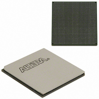
EP3SL150F1152C2N Altera, EP3SL150F1152C2N Datasheet - Page 264

EP3SL150F1152C2N
Manufacturer Part Number
EP3SL150F1152C2N
Description
IC STRATX III FPGA 150K 1152FBGA
Manufacturer
Altera
Series
Stratix® IIIr
Datasheets
1.EP3SL150F780C4N.pdf
(16 pages)
2.EP3SL150F780C4N.pdf
(332 pages)
3.EP3SL150F780C4N.pdf
(456 pages)
Specifications of EP3SL150F1152C2N
Number Of Logic Elements/cells
142500
Number Of Labs/clbs
5700
Total Ram Bits
6390
Number Of I /o
744
Voltage - Supply
0.86 V ~ 1.15 V
Mounting Type
Surface Mount
Operating Temperature
0°C ~ 85°C
Package / Case
1152-FBGA
For Use With
544-2568 - KIT DEVELOPMENT STRATIX III
Lead Free Status / RoHS Status
Lead free / RoHS Compliant
Number Of Gates
-
Other names
544-2409
EP3SL150F1152C2NES
EP3SL150F1152C2NES
Available stocks
Company
Part Number
Manufacturer
Quantity
Price
Part Number:
EP3SL150F1152C2N
Manufacturer:
ALTERA
Quantity:
20 000
- Current page: 264 of 456
- Download datasheet (7Mb)
8–16
Table 8–4. I/O Sub-Bank Combinations for Stratix III Devices that do not have ×36 Groups to form two ×36 Groups.
Stratix III Device Handbook, Volume 1
780-pin FineLine BGA
1152-pin FineLine BGA EP3SE80, EP3SE110,
1517-pin FineLine BGA EP3SL200, EP3SE260, and
1760-pin FineLine BGA
(1)
Notes to
(1) This device supports ×36 DQ/DQS groups on the top and bottom I/O banks natively.
(2) You can combine the ×16/×18 DQ/DQS groups from I/O banks 1A and 1C, 2A and 2C, 5A and 5C, 6A and 6C. However, this process is
discouraged because of the size of the package. Similarly, crossing a bank number (for example combining groups from I/O banks 6C and 5C)
is not supported in this package.
Package
Table
8–4:
1
vertical migration with the ×36 emulation implementation, check if migration is
possible by enabling device migration in the Quartus II project.
possible I/O sub-bank combinations to form two ×36 groups. On Stratix III devices
that do not have ×36 groups. Other Stratix III devices in the 1517 - and 1760 - pin
packages support this implementation as well.
Splitting the read or write data bus over more than one device edge is not
recommended.
EP3SL50, EP3SL70,
EP3SE80, EP3SE110,
EP3SL110, EP3SL150,
EP3SL200, and EP3SE260
EP3SL110, EP3SL150,
EP3SL200, EP3SE260, and
EP3SL340
EP3SL340
EP3SL340
Device
■
■
■
■
■
■
■
■
■
■
■
■
■
■
■
■
■
■
■
■
■
■
■
■
1A and 2A
5A and 6A
3A and 4A
7A and 8A
1A and 1C
2A and 2C
3A and 3B
4A and 4B
5A and 5C
6A and 6C
7A and 7B
8A and 8B
1A and 1B
2A and 2B or 1B and 1C
2B and 2C
5A and 5B
6A and 6B or 5B and 5C
6B and 6C
1A and 1B
2A and 2B or 1B and 1C
2B and 2C
5A and 5B
6A and 6B or 5B and 5C
6B and 6C
Chapter 8: External Memory Interfaces in Stratix III Devices
(2)
(2)
(2)
(2)
I/O Sub-Bank Combinations
© March 2010 Altera Corporation
Memory Interfaces Pin Support
Table 8–4
shows the
Related parts for EP3SL150F1152C2N
Image
Part Number
Description
Manufacturer
Datasheet
Request
R

Part Number:
Description:
CYCLONE II STARTER KIT EP2C20N
Manufacturer:
Altera
Datasheet:

Part Number:
Description:
CPLD, EP610 Family, ECMOS Process, 300 Gates, 16 Macro Cells, 16 Reg., 16 User I/Os, 5V Supply, 35 Speed Grade, 24DIP
Manufacturer:
Altera Corporation
Datasheet:

Part Number:
Description:
CPLD, EP610 Family, ECMOS Process, 300 Gates, 16 Macro Cells, 16 Reg., 16 User I/Os, 5V Supply, 15 Speed Grade, 24DIP
Manufacturer:
Altera Corporation
Datasheet:

Part Number:
Description:
Manufacturer:
Altera Corporation
Datasheet:

Part Number:
Description:
CPLD, EP610 Family, ECMOS Process, 300 Gates, 16 Macro Cells, 16 Reg., 16 User I/Os, 5V Supply, 30 Speed Grade, 24DIP
Manufacturer:
Altera Corporation
Datasheet:

Part Number:
Description:
High-performance, low-power erasable programmable logic devices with 8 macrocells, 10ns
Manufacturer:
Altera Corporation
Datasheet:

Part Number:
Description:
High-performance, low-power erasable programmable logic devices with 8 macrocells, 7ns
Manufacturer:
Altera Corporation
Datasheet:

Part Number:
Description:
Classic EPLD
Manufacturer:
Altera Corporation
Datasheet:

Part Number:
Description:
High-performance, low-power erasable programmable logic devices with 8 macrocells, 10ns
Manufacturer:
Altera Corporation
Datasheet:

Part Number:
Description:
Manufacturer:
Altera Corporation
Datasheet:

Part Number:
Description:
Manufacturer:
Altera Corporation
Datasheet:

Part Number:
Description:
Manufacturer:
Altera Corporation
Datasheet:

Part Number:
Description:
CPLD, EP610 Family, ECMOS Process, 300 Gates, 16 Macro Cells, 16 Reg., 16 User I/Os, 5V Supply, 25 Speed Grade, 24DIP
Manufacturer:
Altera Corporation
Datasheet:


