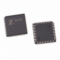
Z85C3008VSG Zilog, Z85C3008VSG Datasheet - Page 168

Z85C3008VSG
Manufacturer Part Number
Z85C3008VSG
Description
IC 8MHZ Z8500 CMOS SCC 44-PLCC
Manufacturer
Zilog
Series
SCCr
Specifications of Z85C3008VSG
Processor Type
Z80
Features
Error Detection and Multiprotocol Support
Speed
8MHz
Voltage
5V
Mounting Type
Surface Mount
Package / Case
44-LCC (J-Lead)
Maximum Operating Temperature
+ 70 C
Minimum Operating Temperature
0 C
Mounting Style
SMD/SMT
Cpu Speed
8MHz
Digital Ic Case Style
LCC
No. Of Pins
44
Supply Voltage Range
5V
Operating Temperature Range
0°C To +70°C
Svhc
No SVHC (18-Jun-2010)
Base Number
85
Rohs Compliant
Yes
Clock Frequency
8MHz
Lead Free Status / RoHS Status
Lead free / RoHS Compliant
Other names
269-3932
Z85C3008VSG
Z85C3008VSG
Available stocks
Company
Part Number
Manufacturer
Quantity
Price
Company:
Part Number:
Z85C3008VSG
Manufacturer:
Zilog
Quantity:
800
Company:
Part Number:
Z85C3008VSG
Manufacturer:
MAX
Quantity:
74
- Current page: 168 of 317
- Download datasheet (4Mb)
UM010901-0601
.
Note: Parameter numbers in this table are the numbers in the Z180 technical manual.
If you are familiar with the Z80 CPU design, the same
interfacing logic applies to the Z180 and I/O interface (see
Figure 9a). This circuit generates /IORD (Read) or IORD
(Write) for peripherals from inputs /IORQ, /RD, and /WR.
The address decodes the Chip Select signal. Note, if you
have Z80 peripherals, the decoder logic decodes only from
addresses (does not have /IORQ). The Z180 signals
/IORQ, /RD, and /WR are active at about the same time
(Parameters #9, 22, 28). However, most of the Z80
peripherals require /CE to /RD or /WR setup time.
No
1
2
3
4
6
9
11
13
15
16
21
22
23
24
25
26a tWRP
27
28
29
Symbol
tcyc
tCHW
tCLW
tcf
tAD
tRDD1
tAH
tRDD2
tDRS
tDRH
tWDZ
tWRD1
tWDD
tWDS
tWRD2
tWDH
tIOD1
tIOD2
Table 5. Z8018010 Timing Parameters for I/O Cycle (Worst Case)
/IORQ
Parameter
Clock Cycle Period
Clock Cycle High Width
Clock Cycle Low Width
Clock Fall Time
Clock High to Address Valid
Clock High to /RD Low IOC=0
Address Hold Time
Clock Low to /RD High
Data to Clock Setup
Data Read Hold Time
Clock High to Data Float Delay
Clock High to /WR Low
Clock Low to Write Data Delay
Write Data Setup to /WR Low
Clock Low to /WR High
/WR Pulse Width (I/O Write)
/WR High to Data Hold Time
Clock High to /IORQ Low IOC=0
Clock Low to /IORQ High
/WR
A17
/RD
A6
A2
A5
A4
A3
Figure 9a. I/O Interface Logic (Example)
G1
/G2A
/G2B
C
B
A
HCT138
/Y9
/Y6
/Y5
/Y4
/Y3
/Y2
/Y1
/Y0
Since the Z180 occupies 64 bytes of I/O addressing space
for system control and on-chip peripherals, there are no
overlapping I/O addresses for off-chip peripherals. In this
design, leave the area as default or assign on-chip
registers at I/O address 0000h to 003Fh.
Figure 9 shows a simple address decoder (the required
interface signals, other than address decode outputs, are
discussed later).
/IORD To Each
Peripherals' /RD
/IOWR To Each
Peripherals' /WR
50 ~
58 ~
54 ~
50 ~
40 ~
48 ~
44 ~
40 ~
Chip Select Signals
for Peripherals
The Z180™ Interfaced with the SCC at MHZ
Min
100
210
40
40
10
25
15
10
0
Max
10
70
55
50
60
50
60
50
55
50
Application Note
Units
ns
ns
ns
ns
ns
ns
ns
ns
ns
ns
ns
ns
ns
ns
ns
ns
ns
ns
ns
6-33
7
Related parts for Z85C3008VSG
Image
Part Number
Description
Manufacturer
Datasheet
Request
R

Part Number:
Description:
Manufacturer:
Zilog, Inc.
Datasheet:

Part Number:
Description:
Cmos Scc Serial Communications Controller
Manufacturer:
ZiLOG Semiconductor
Datasheet:

Part Number:
Description:
Communication Controllers, ZILOG INTELLIGENT PERIPHERAL CONTROLLER (ZIP)
Manufacturer:
Zilog, Inc.
Datasheet:

Part Number:
Description:
KIT DEV FOR Z8 ENCORE 16K TO 64K
Manufacturer:
Zilog
Datasheet:

Part Number:
Description:
KIT DEV Z8 ENCORE XP 28-PIN
Manufacturer:
Zilog
Datasheet:

Part Number:
Description:
DEV KIT FOR Z8 ENCORE 8K/4K
Manufacturer:
Zilog
Datasheet:

Part Number:
Description:
KIT DEV Z8 ENCORE XP 28-PIN
Manufacturer:
Zilog
Datasheet:

Part Number:
Description:
DEV KIT FOR Z8 ENCORE 4K TO 8K
Manufacturer:
Zilog
Datasheet:

Part Number:
Description:
CMOS Z8 microcontroller. ROM 16 Kbytes, RAM 256 bytes, speed 16 MHz, 32 lines I/O, 3.0V to 5.5V
Manufacturer:
Zilog, Inc.
Datasheet:

Part Number:
Description:
Low-cost microcontroller. 512 bytes ROM, 61 bytes RAM, 8 MHz
Manufacturer:
Zilog, Inc.
Datasheet:

Part Number:
Description:
Z8 4K OTP Microcontroller
Manufacturer:
Zilog, Inc.
Datasheet:

Part Number:
Description:
CMOS SUPER8 ROMLESS MCU
Manufacturer:
Zilog, Inc.
Datasheet:

Part Number:
Description:
SL1866 CMOSZ8 OTP Microcontroller
Manufacturer:
Zilog, Inc.
Datasheet:


