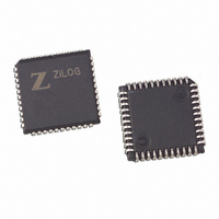
Z85C3008VSG Zilog, Z85C3008VSG Datasheet - Page 77

Z85C3008VSG
Manufacturer Part Number
Z85C3008VSG
Description
IC 8MHZ Z8500 CMOS SCC 44-PLCC
Manufacturer
Zilog
Series
SCCr
Specifications of Z85C3008VSG
Processor Type
Z80
Features
Error Detection and Multiprotocol Support
Speed
8MHz
Voltage
5V
Mounting Type
Surface Mount
Package / Case
44-LCC (J-Lead)
Maximum Operating Temperature
+ 70 C
Minimum Operating Temperature
0 C
Mounting Style
SMD/SMT
Cpu Speed
8MHz
Digital Ic Case Style
LCC
No. Of Pins
44
Supply Voltage Range
5V
Operating Temperature Range
0°C To +70°C
Svhc
No SVHC (18-Jun-2010)
Base Number
85
Rohs Compliant
Yes
Clock Frequency
8MHz
Lead Free Status / RoHS Status
Lead free / RoHS Compliant
Other names
269-3932
Z85C3008VSG
Z85C3008VSG
Available stocks
Company
Part Number
Manufacturer
Quantity
Price
Company:
Part Number:
Z85C3008VSG
Manufacturer:
Zilog
Quantity:
800
Company:
Part Number:
Z85C3008VSG
Manufacturer:
MAX
Quantity:
74
- Current page: 77 of 317
- Download datasheet (4Mb)
SCC™/ESCC™ User’s Manual
Data Communication Modes
4.1 INTRODUCTION (Continued)
For asynchronous data, the Transmit Shift register is for-
matted with start and stop bits along with the data; option-
ally with parity information bit. The formatted character is
shifted out to the transmit multiplexer at the selected clock
rate. WR6 & WR7 are not used in Asynchronous mode.
Synchronous data (except SDLC/HDLC) is shifted to the
CRC generator as well as to the transmit multiplexer.
SDLC/HDLC data is shifted to the CRC Generator and out
through the zero insertion logic (which is disabled while the
flags are being sent). A 0 is inserted in all address, control,
information, and frame check fields following five contigu-
ous 1s in the data stream. The result of the CRC generator
for SDLC data is also routed through the zero insertion log-
ic and then to the transmit multiplexer.
4-2
BRG
Input
RxD
DPLL
Upper Byte (WR13)
IN
Time Constant
16-Bit Down Counter
Notes:
1-Bit
* Not with NMOS.
** Rec. Data FIFO and Rec. Error FIFO are 8 Bytes Deep (ESCC), 3 Bytes Deep (NMOS/CMOS).
DPLL
Internal TXD
MUX
Lower Byte (WR12)
Time Constant
Figure 4-2. Receive Data Path
DPLL
OUT
NRZI Decode
DIV 2
To Transmit Section
Internal Data Bus
SYNC Register
& Zero Delete
BRG
Output
4.1.2 Receive Data Path Description
On the ESCC, the receiver has an 8-byte deep, 8-bit wide
Data FIFO, while the NMOS/CMOS version receiver has a
3-byte deep, 8-bit wide data buffer. In both cases, the Data
buffer is paired with an 8-bit Error FIFO and an 8-bit Shift
Register. The receive data path is shown in Figure 4-2.
This arrangement creates a 8-character buffer, allowing
time for the CPU to service an interrupt or for the DMA to
acquire the bus at the beginning of a block of high-speed
data. It is not necessary to enable the Receive FIFO, since
it is available in all modes of operation. For each data byte
in the Receive FIFO, a byte is loaded into the Error FIFO
to store parity, framing, and other status information. The
Error FIFO is addressed through Read Register 1.
MUX
Note
Hunt Mode (BISYNC)
See
10 x 19 Frame*
14-Bit Counter
Status FIFO
SDLC-CRC
3-Bit
Rec. Data FIFO**
Note
Register (8 bits)
See
I/O Data buffer
Receive Shift
CRC Delay
Register
Checker
CPU I/O
CRC
Rec. Error FIFO**
CRC Result
SYNC
CRC
Note
Rec. Error Logic
See
UM010901-0601
Related parts for Z85C3008VSG
Image
Part Number
Description
Manufacturer
Datasheet
Request
R

Part Number:
Description:
Manufacturer:
Zilog, Inc.
Datasheet:

Part Number:
Description:
Cmos Scc Serial Communications Controller
Manufacturer:
ZiLOG Semiconductor
Datasheet:

Part Number:
Description:
Communication Controllers, ZILOG INTELLIGENT PERIPHERAL CONTROLLER (ZIP)
Manufacturer:
Zilog, Inc.
Datasheet:

Part Number:
Description:
KIT DEV FOR Z8 ENCORE 16K TO 64K
Manufacturer:
Zilog
Datasheet:

Part Number:
Description:
KIT DEV Z8 ENCORE XP 28-PIN
Manufacturer:
Zilog
Datasheet:

Part Number:
Description:
DEV KIT FOR Z8 ENCORE 8K/4K
Manufacturer:
Zilog
Datasheet:

Part Number:
Description:
KIT DEV Z8 ENCORE XP 28-PIN
Manufacturer:
Zilog
Datasheet:

Part Number:
Description:
DEV KIT FOR Z8 ENCORE 4K TO 8K
Manufacturer:
Zilog
Datasheet:

Part Number:
Description:
CMOS Z8 microcontroller. ROM 16 Kbytes, RAM 256 bytes, speed 16 MHz, 32 lines I/O, 3.0V to 5.5V
Manufacturer:
Zilog, Inc.
Datasheet:

Part Number:
Description:
Low-cost microcontroller. 512 bytes ROM, 61 bytes RAM, 8 MHz
Manufacturer:
Zilog, Inc.
Datasheet:

Part Number:
Description:
Z8 4K OTP Microcontroller
Manufacturer:
Zilog, Inc.
Datasheet:

Part Number:
Description:
CMOS SUPER8 ROMLESS MCU
Manufacturer:
Zilog, Inc.
Datasheet:

Part Number:
Description:
SL1866 CMOSZ8 OTP Microcontroller
Manufacturer:
Zilog, Inc.
Datasheet:


