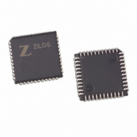
Z85C3008VSG Zilog, Z85C3008VSG Datasheet - Page 76

Z85C3008VSG
Manufacturer Part Number
Z85C3008VSG
Description
IC 8MHZ Z8500 CMOS SCC 44-PLCC
Manufacturer
Zilog
Series
SCCr
Specifications of Z85C3008VSG
Processor Type
Z80
Features
Error Detection and Multiprotocol Support
Speed
8MHz
Voltage
5V
Mounting Type
Surface Mount
Package / Case
44-LCC (J-Lead)
Maximum Operating Temperature
+ 70 C
Minimum Operating Temperature
0 C
Mounting Style
SMD/SMT
Cpu Speed
8MHz
Digital Ic Case Style
LCC
No. Of Pins
44
Supply Voltage Range
5V
Operating Temperature Range
0°C To +70°C
Svhc
No SVHC (18-Jun-2010)
Base Number
85
Rohs Compliant
Yes
Clock Frequency
8MHz
Lead Free Status / RoHS Status
Lead free / RoHS Compliant
Other names
269-3932
Z85C3008VSG
Z85C3008VSG
Available stocks
Company
Part Number
Manufacturer
Quantity
Price
Company:
Part Number:
Z85C3008VSG
Manufacturer:
Zilog
Quantity:
800
Company:
Part Number:
Z85C3008VSG
Manufacturer:
MAX
Quantity:
74
- Current page: 76 of 317
- Download datasheet (4Mb)
UM010901-0601
4.1 INTRODUCTION
The SCC provides two independent, full-duplex channels
programmable for use in any common asynchronous or
synchronous data communication protocol. The data com-
munication protocols handled by the SCC are:
Asynchronous mode:
Asynchronous (x16, x32, or x64 clock
Isochronous (x1 clock)
Character-Oriented mode:
Monosynchronous
Bisynchronous
External Synchronous
Bit-Oriented mode
SDLC/HDLC
SDLC/HDLC Loop
From Receiver
SYNC
5-Bit Delay
CRC-SDLC
CRC-Gen
WR7
Insert
Zero
Register
20-Bit TX Shift Register
SYNC
Internal Data Bus
Figure 4-1. Transmit Data Path
WR6
Register
ASYNC
SYNC
SDLC
MUX & 2-Bit
WR8
Transmit
Delay
U
C
D
Transmit Clock
4.1.1 Transmit Data Path Description
A diagram of the transmit data path is shown in Figure 4-1.
The transmitter has a Transmit Data buffer (a 4-byte deep
FIFO on the ESCC, a one byte deep buffer on the
NMOS/CMOS version) which is addressed through WR8.
It is not necessary to enable the transmit buffer. It is
available in all modes of operation. The Transmit Shift
register is loaded from either WR6, WR7, or the Transmit
Data buffer. In Synchronous modes, WR6 and WR7 are
programmed with the sync characters. In Monosync mode,
an 8-bit or 6-bit sync character is used (WR6), whereas a
16-bit sync character is used in the Bisynchronous mode
(WR6 and WR7). In bit-oriented Synchronous modes, the
SDLC flag character (7E hex) is programmed in WR7 and
is loaded into the Transmit Shift Register at the beginning
and end of each message.
SER
ATA
HAPTER
TX Buffer (1-Byte; NMOS/CMOS)
TX FIFO (4 Byte; ESCC)
’
S
C
M
OMMUNICATION
ANUAL
Internal TxD
Final TX
Encode
NRZI
MUX
4
To Other Channel
TxD
M
ODES
4-1
4
Related parts for Z85C3008VSG
Image
Part Number
Description
Manufacturer
Datasheet
Request
R

Part Number:
Description:
Manufacturer:
Zilog, Inc.
Datasheet:

Part Number:
Description:
Cmos Scc Serial Communications Controller
Manufacturer:
ZiLOG Semiconductor
Datasheet:

Part Number:
Description:
Communication Controllers, ZILOG INTELLIGENT PERIPHERAL CONTROLLER (ZIP)
Manufacturer:
Zilog, Inc.
Datasheet:

Part Number:
Description:
KIT DEV FOR Z8 ENCORE 16K TO 64K
Manufacturer:
Zilog
Datasheet:

Part Number:
Description:
KIT DEV Z8 ENCORE XP 28-PIN
Manufacturer:
Zilog
Datasheet:

Part Number:
Description:
DEV KIT FOR Z8 ENCORE 8K/4K
Manufacturer:
Zilog
Datasheet:

Part Number:
Description:
KIT DEV Z8 ENCORE XP 28-PIN
Manufacturer:
Zilog
Datasheet:

Part Number:
Description:
DEV KIT FOR Z8 ENCORE 4K TO 8K
Manufacturer:
Zilog
Datasheet:

Part Number:
Description:
CMOS Z8 microcontroller. ROM 16 Kbytes, RAM 256 bytes, speed 16 MHz, 32 lines I/O, 3.0V to 5.5V
Manufacturer:
Zilog, Inc.
Datasheet:

Part Number:
Description:
Low-cost microcontroller. 512 bytes ROM, 61 bytes RAM, 8 MHz
Manufacturer:
Zilog, Inc.
Datasheet:

Part Number:
Description:
Z8 4K OTP Microcontroller
Manufacturer:
Zilog, Inc.
Datasheet:

Part Number:
Description:
CMOS SUPER8 ROMLESS MCU
Manufacturer:
Zilog, Inc.
Datasheet:

Part Number:
Description:
SL1866 CMOSZ8 OTP Microcontroller
Manufacturer:
Zilog, Inc.
Datasheet:


