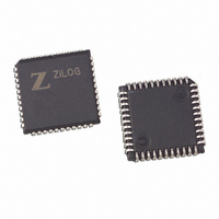
Z85C3008VSG Zilog, Z85C3008VSG Datasheet - Page 178

Z85C3008VSG
Manufacturer Part Number
Z85C3008VSG
Description
IC 8MHZ Z8500 CMOS SCC 44-PLCC
Manufacturer
Zilog
Series
SCCr
Specifications of Z85C3008VSG
Processor Type
Z80
Features
Error Detection and Multiprotocol Support
Speed
8MHz
Voltage
5V
Mounting Type
Surface Mount
Package / Case
44-LCC (J-Lead)
Maximum Operating Temperature
+ 70 C
Minimum Operating Temperature
0 C
Mounting Style
SMD/SMT
Cpu Speed
8MHz
Digital Ic Case Style
LCC
No. Of Pins
44
Supply Voltage Range
5V
Operating Temperature Range
0°C To +70°C
Svhc
No SVHC (18-Jun-2010)
Base Number
85
Rohs Compliant
Yes
Clock Frequency
8MHz
Lead Free Status / RoHS Status
Lead free / RoHS Compliant
Other names
269-3932
Z85C3008VSG
Z85C3008VSG
Available stocks
Company
Part Number
Manufacturer
Quantity
Price
Company:
Part Number:
Z85C3008VSG
Manufacturer:
Zilog
Quantity:
800
Company:
Part Number:
Z85C3008VSG
Manufacturer:
MAX
Quantity:
74
- Current page: 178 of 317
- Download datasheet (4Mb)
UM010901-0601
The primary chip in this logic is the Shift register (HCT164),
which generates /INTACK, /SCCRD and /WAIT. During
I/O and normal memory access cycles, the Shift Register
(HCT164) remains cleared because the /M1 signal is
inactive during the opcode fetch cycle. Since the Shift
Register output is Low, control of /SCCRD and /WAIT is by
Normally, an Interrupt Acknowledge cycle appears from
the Z180 during /M1 and /IORQ active (which is detected
on the third rising edge of PHI after T1). To get an early
sign of an Interrupt Acknowledge cycle, the Shift register
decodes an active /M1. This is during the presence of an
inactive /MREQ on the rising edge of T2.
During an Interrupt Acknowledge cycle, the /INTACK
signal is generated on the rising edge of T2. Since it is the
presence of /INTACK and an active SCCRD that gates the
interrupt vector onto the data bus, the logic also generates
/SCCRD at the proper time. The timing parameter of
concern
USING EPLD
Figure 16a and Figure 16b show the logic using either
EPLD or the circuit of this system. The EPLD is ALTERA
610 which is a 24-Pin EPLD. The method to convert
here
VECTOR
/INTACK
/SCCRD
/IORQ
/WAIT
/M1
is
TdIAi(RD)
10
T1
Figure 15. SCC Interrupt Acknowledge Cycle Timing
60 ns max
[/INTACK
SCC
T2
15
to
T
WA
28
/RD
SCC
50 ns max
13
other system logic and gated through the NOR gate
(HCT27). During I/O and normal memory access cycles,
/SCCRD and /SCCWR are generated from the system /RD
and /WR signals, respectively. The generation is by the
logic at the top of Figure 15.
(Acknowledge) Low delay]. This time delay allows the
interrupt daisy chain to settle so the device requesting the
interrupt places its interrupt vector onto the data bus.
The Shift Register allows enough time delay from the
generation of /INTACK before it generates /SCCRD.
During this delay, it places the Z180 into a Wait state until
the valid interrupt vector is placed onto the data bus. If the
time between these two signals is not enough for daisy
chain settling, more time is added by taking /SCCRD and
/WAIT from a later position on the Shift Register. If there is
a requirement for more wait states, the time is calculated
by PHI cycles.
random gate logic to EPLD is to disassemble MSIs’ logic
into SSI level, and then simplify the logic.
T WA
120 ns max
The Z180™ Interfaced with the SCC at MHZ
T WA
SCC
10
60 ns max
T WA
50 ns max
Valid Data
15
14
29
T3
> 25 ns
Application Note
6-43
7
Related parts for Z85C3008VSG
Image
Part Number
Description
Manufacturer
Datasheet
Request
R

Part Number:
Description:
Manufacturer:
Zilog, Inc.
Datasheet:

Part Number:
Description:
Cmos Scc Serial Communications Controller
Manufacturer:
ZiLOG Semiconductor
Datasheet:

Part Number:
Description:
Communication Controllers, ZILOG INTELLIGENT PERIPHERAL CONTROLLER (ZIP)
Manufacturer:
Zilog, Inc.
Datasheet:

Part Number:
Description:
KIT DEV FOR Z8 ENCORE 16K TO 64K
Manufacturer:
Zilog
Datasheet:

Part Number:
Description:
KIT DEV Z8 ENCORE XP 28-PIN
Manufacturer:
Zilog
Datasheet:

Part Number:
Description:
DEV KIT FOR Z8 ENCORE 8K/4K
Manufacturer:
Zilog
Datasheet:

Part Number:
Description:
KIT DEV Z8 ENCORE XP 28-PIN
Manufacturer:
Zilog
Datasheet:

Part Number:
Description:
DEV KIT FOR Z8 ENCORE 4K TO 8K
Manufacturer:
Zilog
Datasheet:

Part Number:
Description:
CMOS Z8 microcontroller. ROM 16 Kbytes, RAM 256 bytes, speed 16 MHz, 32 lines I/O, 3.0V to 5.5V
Manufacturer:
Zilog, Inc.
Datasheet:

Part Number:
Description:
Low-cost microcontroller. 512 bytes ROM, 61 bytes RAM, 8 MHz
Manufacturer:
Zilog, Inc.
Datasheet:

Part Number:
Description:
Z8 4K OTP Microcontroller
Manufacturer:
Zilog, Inc.
Datasheet:

Part Number:
Description:
CMOS SUPER8 ROMLESS MCU
Manufacturer:
Zilog, Inc.
Datasheet:

Part Number:
Description:
SL1866 CMOSZ8 OTP Microcontroller
Manufacturer:
Zilog, Inc.
Datasheet:


