Z85C3008VSG Zilog, Z85C3008VSG Datasheet - Page 83
Z85C3008VSG
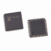
Manufacturer Part Number
Z85C3008VSG
Description
IC 8MHZ Z8500 CMOS SCC 44-PLCC
Manufacturer
Zilog
Series
SCCr
Specifications of Z85C3008VSG
Processor Type
Z80
Features
Error Detection and Multiprotocol Support
Speed
8MHz
Voltage
5V
Mounting Type
Surface Mount
Package / Case
44-LCC (J-Lead)
Maximum Operating Temperature
+ 70 C
Minimum Operating Temperature
0 C
Mounting Style
SMD/SMT
Cpu Speed
8MHz
Digital Ic Case Style
LCC
No. Of Pins
44
Supply Voltage Range
5V
Operating Temperature Range
0°C To +70°C
Svhc
No SVHC (18-Jun-2010)
Base Number
85
Rohs Compliant
Yes
Clock Frequency
8MHz
Lead Free Status / RoHS Status
Lead free / RoHS Compliant
Other names
269-3932
Z85C3008VSG
Z85C3008VSG
Available stocks
Company
Part Number
Manufacturer
Quantity
Price
Company:

Part Number:
Z85C3008VSG
Manufacturer:
Zilog
Quantity:
800
Company:
Part Number:
Z85C3008VSG
Manufacturer:
MAX
Quantity:
74


SCC™/ESCC™ User’s Manual
Data Communication Modes
4.3 BYTE-ORIENTED SYNCHRONOUS MODE
The SCC supports three byte-oriented synchronous proto-
cols. They are: monosynchronous, bisynchronous, and ex-
ternal synchronous.
In synchronous communications, the bit cell boundaries
are referenced to a clock signal common to both the trans-
mitter and receiver. Consequently, they operate in a fixed-
phase relationship. This eliminates the need for the receiv-
er to locate the bit cell boundaries with a clock 16, 32, or
64 times the receive data rate, allowing for higher speed
communication links. Some applications may encode (i.e.,
NRZI or FM coding) the clock information on the same line
as the data. Therefore, these applications require that the
receiver use a high speed clock to find the bit cell bound-
aries (decoding is typically done with the PLL—Phase-
Locked Loop; the SCC has on-chip Digital PLL). Data en-
coding eliminates the need to transmit the synchronous
clock on a separate wire from the data.
Synchronous data does not use start and stop bits to de-
lineate the boundaries for each character. This eliminates
the overhead associated with every character and increas-
es the line efficiency. Because of the phase relationship of
synchronous data to a clock, data is transferred in blocks
4.3.1 Byte-Oriented Synchronous Transmit
Once Synchronous mode has been selected, any of three
of the following sync character lengths may be selected:
The 6-bit option sync character is selected by setting bits
4 and 5 of WR4 to zeros and bit 0 of WR10 to one. Only
the least significant six bits of WR6 are transmitted.
4-8
6-bit
8-bit
16-bit
Modem Clock
Bit State
Data
Bit
LSB
Figure 4-4. Monosync Data Character Format
0
1
1 1 0
2 3 4
Sync Character
1 0
5 6
1 Bit Time
0 0
7 8
with no gaps between characters. This requires that there
be an agreement as to the location of the character
boundaries so that the characters can be properly
framed. This is normally accomplished by defining spe-
cial synchronization patterns, or Sync characters. The
synchronization pattern serves as a reference; it signals
the receiver that a character boundary occurs immediate-
ly after the last bit of the pattern. For example Monosync
Protocol usually uses 16 Hex as this special character,
and the SDLC protocol uses 0, six 1s, followed by a 0 (7E
Hex; usually referred to as Flag Pattern) to mark the be-
ginning and end of a block of data. Another way of iden-
tifying the character boundaries (i.e., achieving synchro-
nization) is with a logic signal that goes active just as the
first character is about to enter the receiver. This method
is referred to as External Synchronization.
Figure 4-4 shows the character format for synchronous
transmission. For example, bits 1-8 might be one charac-
ter and bits 9-13 part of another character; or, bit 1 might
be part of a second character, and bits 10-13 part of a third
character. This is accomplished by defining a synchroniza-
tion character, commonly called a Sync Character.
The 8-bit sync character is selected by setting bits 4 and 5
of WR4 to zeros and bit 0 of WR10 to zeros. With this op-
tion selected, the transmitter sends the contents of WR6
when it has no data to send.
For a 16-bit sync character, set bit D4 of WR4 to 1 and bit
D5 of WR4 and bit D0 of WR10 to 0. In this mode, the
transmitter sends the concatenation of WR6 and WR7 for
the idle line condition.
Because the receiver requires that sync characters be left-
justified in the registers, while the transmitter requires
them to be right justified, only the receiver works with a 12-
bit sync character. While the receiver is in External Sync
1 1
9 10 11 12 13 . . .
0 1
Data Character
0 1
0 1
UM010901-0601
Related parts for Z85C3008VSG
Image
Part Number
Description
Manufacturer
Datasheet
Request
R

Part Number:
Description:
Manufacturer:
Zilog, Inc.
Datasheet:

Part Number:
Description:
Cmos Scc Serial Communications Controller
Manufacturer:
ZiLOG Semiconductor
Datasheet:
Part Number:
Description:
Communication Controllers, ZILOG INTELLIGENT PERIPHERAL CONTROLLER (ZIP)
Manufacturer:
Zilog, Inc.
Datasheet:

Part Number:
Description:
KIT DEV FOR Z8 ENCORE 16K TO 64K
Manufacturer:
Zilog
Datasheet:

Part Number:
Description:
KIT DEV Z8 ENCORE XP 28-PIN
Manufacturer:
Zilog
Datasheet:

Part Number:
Description:
DEV KIT FOR Z8 ENCORE 8K/4K
Manufacturer:
Zilog
Datasheet:

Part Number:
Description:
KIT DEV Z8 ENCORE XP 28-PIN
Manufacturer:
Zilog
Datasheet:

Part Number:
Description:
DEV KIT FOR Z8 ENCORE 4K TO 8K
Manufacturer:
Zilog
Datasheet:
Part Number:
Description:
CMOS Z8 microcontroller. ROM 16 Kbytes, RAM 256 bytes, speed 16 MHz, 32 lines I/O, 3.0V to 5.5V
Manufacturer:
Zilog, Inc.
Datasheet:
Part Number:
Description:
Low-cost microcontroller. 512 bytes ROM, 61 bytes RAM, 8 MHz
Manufacturer:
Zilog, Inc.
Datasheet:
Part Number:
Description:
Z8 4K OTP Microcontroller
Manufacturer:
Zilog, Inc.
Datasheet:
Part Number:
Description:
CMOS SUPER8 ROMLESS MCU
Manufacturer:
Zilog, Inc.
Datasheet:
Part Number:
Description:
SL1866 CMOSZ8 OTP Microcontroller
Manufacturer:
Zilog, Inc.
Datasheet: