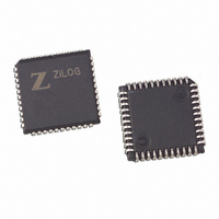
Z85C3008VSG Zilog, Z85C3008VSG Datasheet - Page 90

Z85C3008VSG
Manufacturer Part Number
Z85C3008VSG
Description
IC 8MHZ Z8500 CMOS SCC 44-PLCC
Manufacturer
Zilog
Series
SCCr
Specifications of Z85C3008VSG
Processor Type
Z80
Features
Error Detection and Multiprotocol Support
Speed
8MHz
Voltage
5V
Mounting Type
Surface Mount
Package / Case
44-LCC (J-Lead)
Maximum Operating Temperature
+ 70 C
Minimum Operating Temperature
0 C
Mounting Style
SMD/SMT
Cpu Speed
8MHz
Digital Ic Case Style
LCC
No. Of Pins
44
Supply Voltage Range
5V
Operating Temperature Range
0°C To +70°C
Svhc
No SVHC (18-Jun-2010)
Base Number
85
Rohs Compliant
Yes
Clock Frequency
8MHz
Lead Free Status / RoHS Status
Lead free / RoHS Compliant
Other names
269-3932
Z85C3008VSG
Z85C3008VSG
Available stocks
Company
Part Number
Manufacturer
Quantity
Price
Company:
Part Number:
Z85C3008VSG
Manufacturer:
Zilog
Quantity:
800
Company:
Part Number:
Z85C3008VSG
Manufacturer:
MAX
Quantity:
74
- Current page: 90 of 317
- Download datasheet (4Mb)
UM010901-0601
Modem Controls. Up to two modem control signals asso-
ciated with the receiver are available in Synchronous
modes: /DTR//REQ and /DCD. The /DTR//REQ pin carries
the inverted state of the DTR bit (D7) in WR5 unless this
pin has been programmed to carry a DMA Request on
Transmit signal. The /DCD pin is ordinarily a simple input
to the DCD bit in RR0. However, if the Auto Enables mode
is selected by setting D5 of WR3 to 1, this pin becomes an
enable for the receiver. Therefore, if Auto Enables is ON
and the /DCD pin is High, the receiver is disabled; while
the /DCD pin is Low, the receiver is enabled.
Note that with Auto Enables mode enabled, when /DCD
goes inactive, the receiver stops immediately and the
character being assembled is lost.
Initialization. The initialization sequence for the receiver
in character-oriented mode is WR4 first, to select the
mode, then WR10 to modify it if necessary; WR6 and WR7
to program the sync characters; WR3 and WR5 to select
the various options. At this point the other registers are ini-
tialized as necessary. When all this is completed, the re-
ceiver is enabled by setting bit D0 of WR3 to a one. A sum-
mary is shown in Table 4-8. A detailed example of using
the SCC in 16-bit sync mode is available in the application
note “SCC in Binary Synchronous Communications.”
SCC™/ESCC™ User’s Manual
Data Communication Modes
4-15
4
Related parts for Z85C3008VSG
Image
Part Number
Description
Manufacturer
Datasheet
Request
R

Part Number:
Description:
Manufacturer:
Zilog, Inc.
Datasheet:

Part Number:
Description:
Cmos Scc Serial Communications Controller
Manufacturer:
ZiLOG Semiconductor
Datasheet:

Part Number:
Description:
Communication Controllers, ZILOG INTELLIGENT PERIPHERAL CONTROLLER (ZIP)
Manufacturer:
Zilog, Inc.
Datasheet:

Part Number:
Description:
KIT DEV FOR Z8 ENCORE 16K TO 64K
Manufacturer:
Zilog
Datasheet:

Part Number:
Description:
KIT DEV Z8 ENCORE XP 28-PIN
Manufacturer:
Zilog
Datasheet:

Part Number:
Description:
DEV KIT FOR Z8 ENCORE 8K/4K
Manufacturer:
Zilog
Datasheet:

Part Number:
Description:
KIT DEV Z8 ENCORE XP 28-PIN
Manufacturer:
Zilog
Datasheet:

Part Number:
Description:
DEV KIT FOR Z8 ENCORE 4K TO 8K
Manufacturer:
Zilog
Datasheet:

Part Number:
Description:
CMOS Z8 microcontroller. ROM 16 Kbytes, RAM 256 bytes, speed 16 MHz, 32 lines I/O, 3.0V to 5.5V
Manufacturer:
Zilog, Inc.
Datasheet:

Part Number:
Description:
Low-cost microcontroller. 512 bytes ROM, 61 bytes RAM, 8 MHz
Manufacturer:
Zilog, Inc.
Datasheet:

Part Number:
Description:
Z8 4K OTP Microcontroller
Manufacturer:
Zilog, Inc.
Datasheet:

Part Number:
Description:
CMOS SUPER8 ROMLESS MCU
Manufacturer:
Zilog, Inc.
Datasheet:

Part Number:
Description:
SL1866 CMOSZ8 OTP Microcontroller
Manufacturer:
Zilog, Inc.
Datasheet:


